IN Brief:
- Rice University researchers have developed an automated workflow for measuring microscopic defects in advanced semiconductors.
- The Python-based tool analyses high-resolution X-ray diffraction data to identify dislocations and calculate defect density.
- Faster crystal-quality assessment could support diamond, GaN, quantum devices, RF systems, and high-power electronics.
Rice University researchers have developed an automated workflow for measuring microscopic defects in diamond and other advanced semiconductor materials.
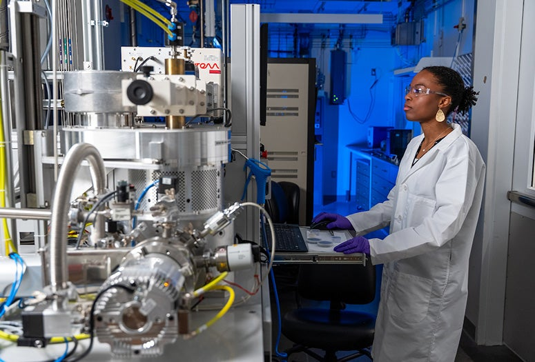
The method uses a custom Python-based software tool to analyse high-resolution X-ray diffraction data. The software examines diffraction patterns, identifies dislocations and irregularities in the atomic lattice, and calculates defect density in the material being measured.
The work is especially suited to diamond and other wide-bandgap semiconductors. These materials can tolerate higher heat and electrical stress than silicon, making them attractive for electric vehicle power systems, power-grid infrastructure, RF communications, and quantum technologies. Their device performance, however, depends heavily on crystal quality.
Dislocations can disrupt charge transport, heat flow, device efficiency, reliability, and manufacturability. Measuring those defects quickly and reproducibly has remained a difficult part of advanced materials development. Existing methods can be slow, labour-intensive, or difficult to scale, particularly when applied to diamond.
The Rice team tested the workflow on four commercially available grades of single-crystal diamond with different expected levels of crystal quality. The automated method distinguished between the materials, identifying electronic-grade diamond as having the lowest defect density and the most uniform crystal quality. Heteroepitaxial diamond, grown on a non-diamond substrate, showed the highest defect density and greatest structural disorder.
The researchers also applied the workflow to gallium nitride, demonstrating that the approach can be adapted across different crystal structures and growth platforms. GaN is already used in power electronics and RF devices, while diamond remains a candidate for next-generation high-power, high-frequency, and quantum systems.
Wide-bandgap semiconductor development is constrained by material reproducibility as much as by device design. A material may have attractive theoretical properties, but it cannot move into demanding electronics applications unless defects can be measured, reduced, and controlled across production batches.
That pressure connects with broader efforts to improve advanced semiconductor materials. Returnable in-space manufacturing work at Space Forge is exploring whether semiconductor crystals can be produced with fewer defects and greater uniformity under microgravity conditions. In terrestrial manufacturing, photonic chip pilot-line work in Eindhoven is placing metrology and process control at the centre of the transition from laboratory devices to repeatable production.
Diamond is a demanding material to qualify. It offers high thermal conductivity, a wide bandgap, high breakdown field, and potential use in quantum technologies, but device-grade material is difficult to produce consistently. Small variations in crystal quality can affect power devices, RF components, and quantum structures where defects alter electrical, thermal, or optical behaviour.
Automating high-resolution X-ray diffraction analysis could reduce one of the bottlenecks in the qualification process. Researchers and manufacturers would be able to compare growth conditions, suppliers, wafer regions, and process changes more quickly. That feedback can help isolate whether a performance issue comes from design, processing, or the starting material.
The software-based approach also improves reproducibility. Manual interpretation can introduce variation between users, laboratories, and sample sets. A consistent computational workflow provides a clearer baseline for comparing material quality, particularly as the method is extended to additional materials, structures, and defect classes.
If the workflow moves into routine laboratory and pre-production use, it could support a more disciplined route for moving diamond and other wide-bandgap semiconductors from promising materials into reliable electronic and quantum devices. Faster defect evaluation will not solve every manufacturing challenge, but it can shorten the feedback loop between crystal growth, process development, and device performance.