IN Brief:
- Researchers deposited less than 10nm of magnesium onto p-type GaN before annealing it at 600°C for five minutes.
- The process achieved specific contact resistivity of roughly 1–3 × 10⁻⁴ Ω·cm² while retaining the thin GaN surface.
- Tests on 50nm p-GaN and p-i-n diodes retained high hole mobility and more than 800V reverse blocking capability.
Nagoya University researchers have developed a contact-formation process for thin p-type gallium nitride that uses an ultrathin magnesium film and brief thermal treatment to reduce electrical resistance without significantly roughening the semiconductor surface. The work addresses a difficult interface in GaN LEDs, transistors, and power devices.
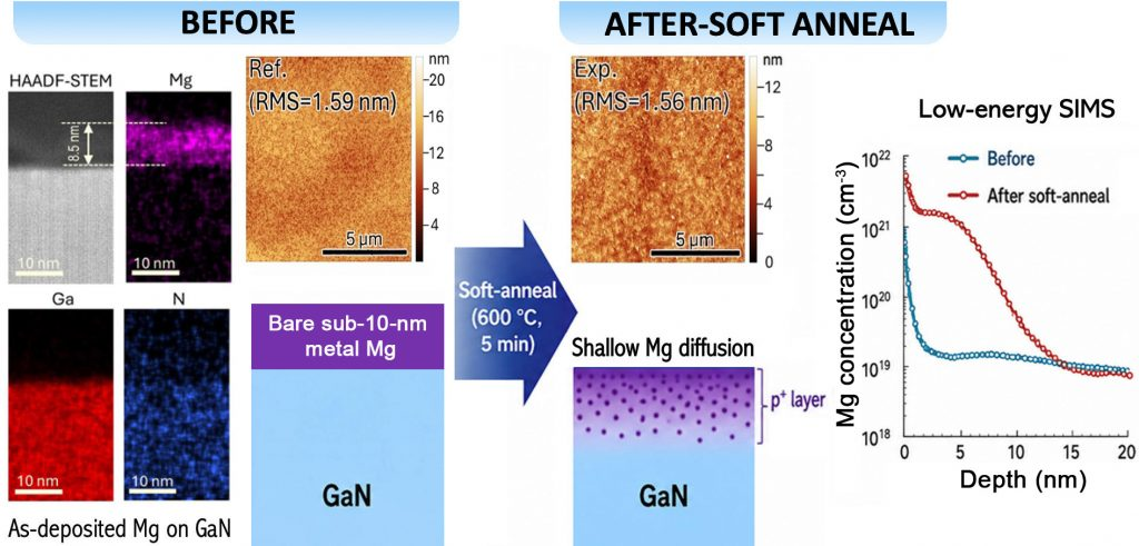
The team deposited an 8–9nm metallic magnesium layer onto p-type GaN and annealed the structure at 600°C for five minutes without using a protective cap layer. It achieved specific contact resistivity of approximately 1–3 × 10⁻⁴ Ω·cm², including on material subjected to plasma processing.
Low-resistance ohmic contacts are necessary because the performance of a semiconductor device is partly determined by how effectively current can pass between its active material and external conductors. Excessive interface resistance produces voltage drop and heat, reducing the benefit gained from improvements elsewhere in the device structure.
The problem is particularly difficult in p-type GaN. Magnesium is widely used as the acceptor dopant, but only a proportion of the dopant contributes mobile holes at room temperature. The comparatively low hole concentration creates a wide depletion region at the metal-semiconductor interface, making it more difficult for carriers to cross the contact efficiently.
Increasing the magnesium concentration immediately beneath the contact can narrow that region and make carrier tunnelling easier. Previous approaches using thicker magnesium layers, however, required heavier thermal processing and risked roughening the surface or creating additional reaction phases — both undesirable when the underlying p-GaN itself may only be tens of nanometres thick.
The Nagoya process reduces both the quantity of deposited magnesium and the thermal load. Measurements showed that magnesium was concentrated in an extremely shallow region near the surface, reaching about 1 × 1021cm-3 before falling rapidly within roughly 10nm. This heavily doped surface region alters the band bending and depletion width at the metal-semiconductor interface.
High-resolution microscopy did not identify the additional crystalline reaction phase associated with some thicker-magnesium processes, while the surface remained comparatively flat. The team also obtained low contact resistance regardless of whether the surface had previously been exposed to plasma processing, increasing the potential compatibility with practical semiconductor fabrication sequences.
The researchers tested the process on p-type GaN layers only 50nm thick and reported that high hole mobility was retained. Applied to p-i-n diodes, the same treatment preserved reverse blocking capability above 800V together with low reverse leakage current.
Those results are important because a contact process that reduces interface resistance while degrading the semiconductor beneath it merely exchanges one electrical problem for another. High-voltage GaN devices depend on maintaining material quality, junction behaviour, and electric-field control at the same time as reducing conduction losses.
The potential applications extend beyond one device family. Thin p-GaN appears in LEDs and micro-LEDs, p-GaN-gate normally-off HEMTs, heterojunction bipolar transistor structures, and vertical GaN power devices. Each architecture imposes different demands on contact geometry and current density, but all can be limited by the difficulty of forming a low-resistance electrical connection to a thin p-type layer.
The process also avoids several manufacturing complications. It does not require a cap layer over the reactive magnesium film, and the anneal is shorter and cooler than the more aggressive processing used in earlier work. Those characteristics do not establish high-volume manufacturability, but they reduce the number of additional process steps that would have to be accommodated in an existing device flow.
Wafer-scale uniformity, contact metallisation, thermal cycling, process variation, and long-term reliability remain to be established. A resistivity result obtained on research structures still has to survive lithographic variation, contamination control, packaging, and the repeated electrical and thermal stresses of an operating device.
The work was published in Applied Physics Letters on 11 August, with Nagoya University’s research announcement following on 18 August and its English-language release appearing on 24 August. The useful result lies in the combination: the contact resistance falls without the rough surface, thick reaction layer, or loss of high-voltage behaviour that would otherwise undermine the value of a thin p-GaN structure.