
IN Brief:
- Kyoto University demonstrated ion-implanted SiC JFET operation at 600°C using a new bottom-gate architecture.
- A double-well isolation structure suppresses high-temperature leakage while the bottom gate improves threshold-voltage control.
- Further work includes larger circuits, wafer-scale fabrication, interconnects, and packaging able to survive the same temperatures.
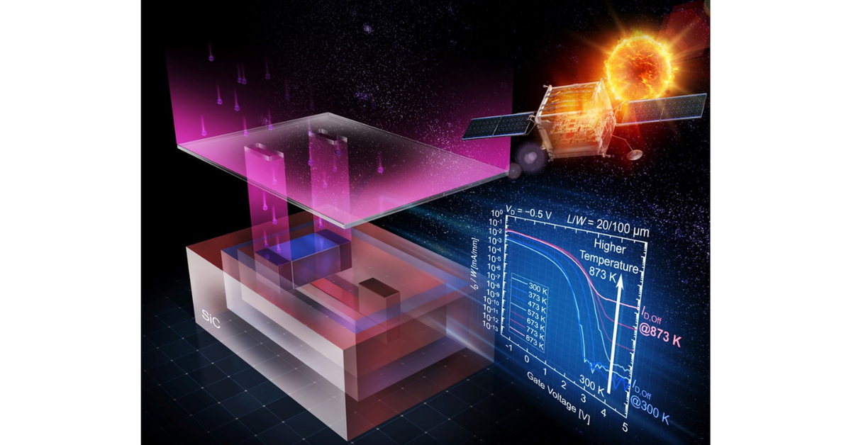
Kyoto University researchers have demonstrated silicon carbide junction field-effect transistors operating at 600°C using a bottom-gate architecture fabricated through ion implantation. The work targets integrated electronics for environments where conventional silicon circuitry cannot operate reliably, including high-temperature machinery and planetary exploration.
The research team, including Mitsuaki Kaneko, Shunya Shibata, and Tsunenobu Kimoto, focused on two limitations of ion-implanted SiC JFETs: threshold-voltage control and leakage at elevated temperature. Earlier top-gate structures made on semi-insulating SiC substrates suffered from variation between intended and measured threshold behaviour, while leakage increased as the operating temperature rose.
The new device places the gate beneath the channel. This changes the way the transistor responds to the channeling tail produced during ion implantation, where a proportion of dopant atoms can penetrate deeper into the crystal than intended. By designing around that profile, the researchers reduced the difference between designed and measured threshold voltage to less than 0.1V at 673K, equivalent to 400°C.
A double-well structure provides electrical isolation. Instead of depending on a semi-insulating substrate to separate devices, the architecture uses pn-junction isolation on an n-type epitaxial layer. The researchers report that this suppresses off-state leakage sufficiently for the JFETs to continue operating at 873K, or 600°C.
Silicon carbide is already well established in high-voltage power electronics, where its wide bandgap and high critical electric field support devices capable of higher voltage and temperature operation than conventional silicon. Integrated logic and control electronics present a different set of difficulties. Circuits need predictable thresholds, reliable isolation, low leakage, stable contacts, and repeatable behaviour across many devices rather than a single switch able to tolerate a hot junction.
The Kyoto work is therefore concerned as much with controllability and fabrication as with the headline temperature. The JFETs were produced using ion implantation, a process familiar to semiconductor manufacturing, rather than an experimental device technique with no obvious route into a broader process flow. That does not make the architecture production-ready, but it removes one potential obstacle to further scaling.
Extreme-temperature circuits could reduce the distance between sensors and their associated signal-processing electronics. Machinery operating around combustion, turbines, furnaces, or other hot processes often keeps conventional electronics away from the heat and connects them through cabling to remote sensors. Electronics that can survive closer to the measurement point could change the mechanical and electrical design of those systems.
Planetary exploration presents a similar problem under more severe constraints. Electronics operating in hostile environments can require substantial thermal protection, adding mass, volume, and power demand. Semiconductor circuits able to function at much higher ambient temperatures could reduce some of that burden, although a transistor demonstration represents only a small part of the complete system required for such an application.
Packaging is one of the remaining barriers. Interconnect metals, dielectrics, contacts, passivation, substrates, bonding systems, and external connections must all survive sustained thermal exposure without unacceptable changes in resistance, mechanical strength, or electrical isolation. A semiconductor channel that continues to operate at 600°C is of limited practical use if the package or interconnect fails at a substantially lower temperature.
The researchers have also identified larger circuits and wafer-scale fabrication as further development areas. Scaling from individual devices to an integrated circuit introduces matching, yield, interconnect, and cumulative leakage problems that may not be apparent from isolated transistor measurements. Process uniformity will become particularly important if threshold control depends on accurately managing implantation profiles and junction geometry.
The work was published in APL Electronic Devices under the title Over 600°C operation of ion-implantation-based SiC bottom-gate JFETs. Its useful result is not simply that SiC can survive extreme heat — that material advantage is already well understood — but that an implanted JFET architecture can retain more predictable threshold behaviour and isolation at temperatures where complete electronic systems remain extremely difficult to build.
