IN Brief:
- The VSMC fab has completed construction and entered risk production after processing its first sample lot at more than 99% yield.
- Processes from 130nm to 40nm will support mixed-signal, analogue, power management, and interposer applications.
- Capacity is planned to reach about 44,000 300mm wafers per month by 2029, with around 1,600 jobs expected at the site.
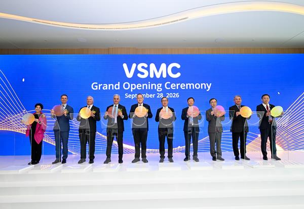
VisionPower Semiconductor Manufacturing Company has opened its first 300mm wafer fab in Tampines, Singapore, with the facility entering risk production ahead of planned volume manufacturing in the first quarter of 2027. VSMC, the joint venture formed by Vanguard International Semiconductor and NXP Semiconductors in 2024, says its first sample lot achieved a yield above 99%.
The fab will support process technologies from 130nm to 40nm for mixed-signal, power management, analogue, and interposer applications serving high performance computing, mobile, automotive, industrial, and consumer markets. The process range places the factory firmly in specialty semiconductor manufacturing rather than leading-edge logic, where voltage handling, analogue performance, embedded functions, reliability, and product longevity can matter more than transistor density.
VSMC’s published technology portfolio includes BCD and ultra-low-power processes alongside embedded-memory options. BCD technologies combine bipolar, CMOS, and DMOS structures and are widely used where control logic has to sit beside higher-voltage analogue or power functions. That makes the platform relevant to power management ICs, motor control, battery systems, interfaces, and other mixed-signal products common in automotive and industrial electronics.
Moving those process families onto 300mm wafers changes the manufacturing economics. A larger wafer can produce more die per process cycle when yield and utilisation are strong, but equipment, mask costs, process complexity, and product mix still determine whether the theoretical area advantage becomes a lower cost per device. Specialty processes also tend to remain in production for long periods, making stable capacity and change control as important as rapid node migration.
Construction took 22 months from the December 2024 groundbreaking. With the cleanroom and production line complete, the factory has now entered risk production, when engineering wafers and early customer material are used to stabilise processes and demonstrate repeatability before higher-volume release. A sample lot yield above 99% is an encouraging early result, but it does not substitute for sustained yield and qualification across the product mix.
The fab uses automated material handling, digital management systems, and AI-assisted manufacturing functions. Those systems can improve traceability and process control across a high-volume wafer operation, while the eventual output still depends on equipment matching, maintenance, statistical process control, defect management, and disciplined recipe control across hundreds of manufacturing steps.
The factory has also been designed against LEED and Singapore Green Mark requirements, with VSMC citing renewable-energy measures, energy efficiency, and water recycling. Those systems are material to a 300mm fab because wafer manufacturing is an intensive user of electricity, ultrapure water, gases, and chemicals, and capacity growth increases the importance of utilities engineering alongside process-tool performance.
At full capacity in 2029, VSMC expects the site to process about 44,000 300mm wafers each month and employ around 1,600 people. The capacity adds another front-end manufacturing source to NXP’s hybrid production model, which combines internal operations with foundry and joint-venture capacity.
That model is also driving investment elsewhere in NXP’s manufacturing chain. The company recently began expanding its Petaling Jaya assembly and test operation in Malaysia, with the new back-end capacity intended to support future output from VSMC in Singapore and the ESMC joint venture in Dresden. Front-end wafer capacity only becomes useful customer supply when assembly, test, qualification, and logistics can scale with it.
The Singapore plant therefore enters production as part of a wider manufacturing network rather than as an isolated fab. Geography can add resilience, but only once qualified process capacity is matched with back-end operations, materials, equipment support, and customer demand. Semiconductor diversification is an operational exercise long before it becomes a supply chain slogan.
Risk production is now the immediate test. VSMC has to translate the first sample lot result into repeatable process capability, complete customer qualification, and ramp a broad set of specialty technologies without compromising yield. Volume production remains scheduled for the first quarter of 2027, leaving the coming months to establish whether the new 300mm line can move from an opened factory to a dependable source of automotive, industrial, and mixed-signal silicon.