IN Brief:
- The 20 kW reference design converts an 800 V DC rack bus directly to a fixed 6 V server rail.
- Two 10 kW modules use Navitas 650 V GaN devices in an input series, output parallel architecture.
- Microchip’s dsPIC33AK controller manages resonant conversion, telemetry, protection, communications and firmware updates.
Microchip Technology and Navitas Semiconductor have developed a 20 kW reference design that converts an 800 V DC rack bus directly to a fixed 6 V server rail, combining high-frequency GaN conversion with digital control and a hardware root of trust.
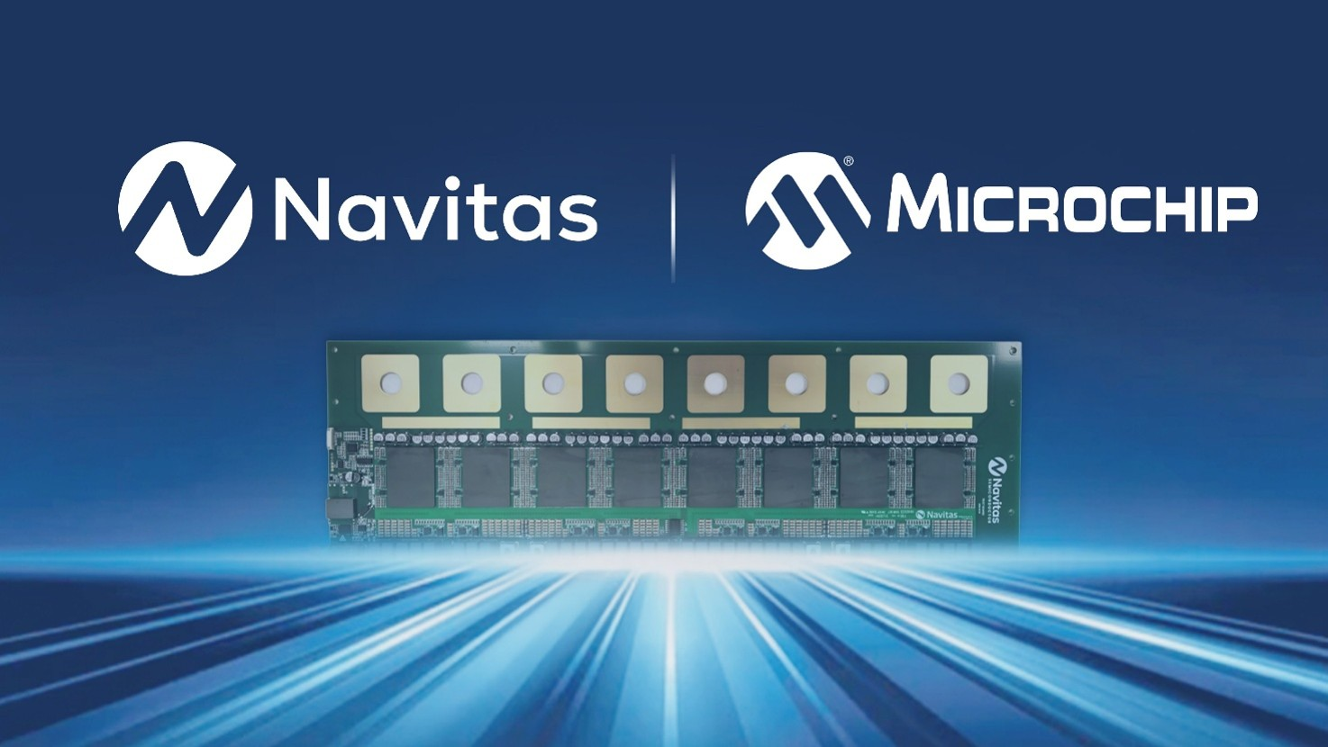
The architecture uses two parallel 10 kW modules in an input series, output parallel configuration around a 128:1 full-bridge LLC topology. Microchip specifies a target efficiency of 96% at approximately 1 MHz, while a 400 × 60 × 6 mm power board, planar transformers and liquid cooling on one side are intended to keep the converter close to the load without consuming the volume associated with a conventional intermediate power shelf.
The design combines functions normally associated with an 800 V-to-50 V stage and a subsequent 50 V-to-6 V stage within one converter. Eliminating the intermediate stage removes a conversion boundary where additional conduction and switching losses, magnetics and control hardware would otherwise be introduced between rack distribution and the low-voltage rail feeding the server electronics.
Navitas supplies 16 NV6034 GaNFast FETs rated at 650 V and 17 mΩ for the primary side, arranged in a stacked half-bridge topology. Their DFN 8 × 8 packages are cooled from both sides, shortening the thermal path from the semiconductor junction into the surrounding cooling structure. At the 1 MHz target switching frequency, switching loss and parasitic inductance become as important as nominal on-resistance because the devices transition between states a million times each second.
The reference platform targets a power density of 2,100 W/in³, while its low profile is intended to allow the power delivery board to sit physically close to the GPU board. Shortening the electrical path between converter and load reduces the inductance through which rapidly changing processor current must be supplied, improving the power system’s ability to respond to steep load transients without excessive voltage excursion.
Microchip’s dsPIC33AK256MPS306 digital signal controller closes the control loop. Its 200 MHz 32-bit core includes a double-precision floating-point unit, high resolution PWM peripherals with 78 ps timing resolution and 12-bit analogue-to-digital converters operating at up to 40 MSPS. Those peripherals allow switching timing and feedback measurements to be handled deterministically rather than relying on a general-purpose processor to manage a resonant power stage.
The controller is also responsible for telemetry, thermal protection, PMBus and SPDM communications and live firmware updating. Microchip provides PLECS models and controller hardware-in-the-loop support around the design so that control strategies and fault behaviour can be exercised before equivalent conditions are applied to the full 800 V hardware.
The control architecture incorporates a TA100 CryptoAuthentication device as a hardware root of trust for secure boot, code authentication, authenticated firmware updates, secure debug and key-management operations. The dsPIC33AK software environment also includes support for algorithms associated with CNSA Suite 2.0 post-quantum guidance.
Joe Thomsen, corporate vice president of Microchip’s digital signal controller business unit, said: “AI infrastructure optimization is driving one of the most significant power architecture transitions the data center industry has experienced in decades. As the ecosystem moves toward higher-voltage rack power systems, developers need proven control and security to help reduce implementation risk. Our collaboration with Navitas combines digital control, hardware-based security and advanced GaN power conversion to help customers bring 800V rack power systems to market more quickly.”
Other 800 V development has extended from rack distribution towards conversion positioned increasingly close to processor boards, with wide-bandgap devices being used to raise switching frequency and reduce the volume occupied by magnetics and passive components. The Microchip and Navitas platform addresses the final conversion to a 6 V rail rather than another intermediate bus.
Vipin Bothra, vice president of global solution marketing at Navitas Semiconductor, said: “As AI infrastructure scales to support increasingly demanding computing platforms, Navitas’ GaNFast technology is a critical enabler of higher power density, greater efficiency and improved system performance. By combining Navitas’ leadership in power semiconductors with Microchip’s digital control expertise, this collaboration accelerates the delivery of advanced power solutions tailored to the evolving requirements of next-generation AI data centers.”
The companies will support the platform with reference hardware, software and design documentation, with design files available through Microchip subject to request and verification. The 20 kW hardware is due to be demonstrated at the OCP Global Summit in San Jose from 12 to 15 October, giving developers a physical implementation against which the thermal, control and conversion behaviour of the direct 800 V-to-6 V architecture can be evaluated.