IN Brief:
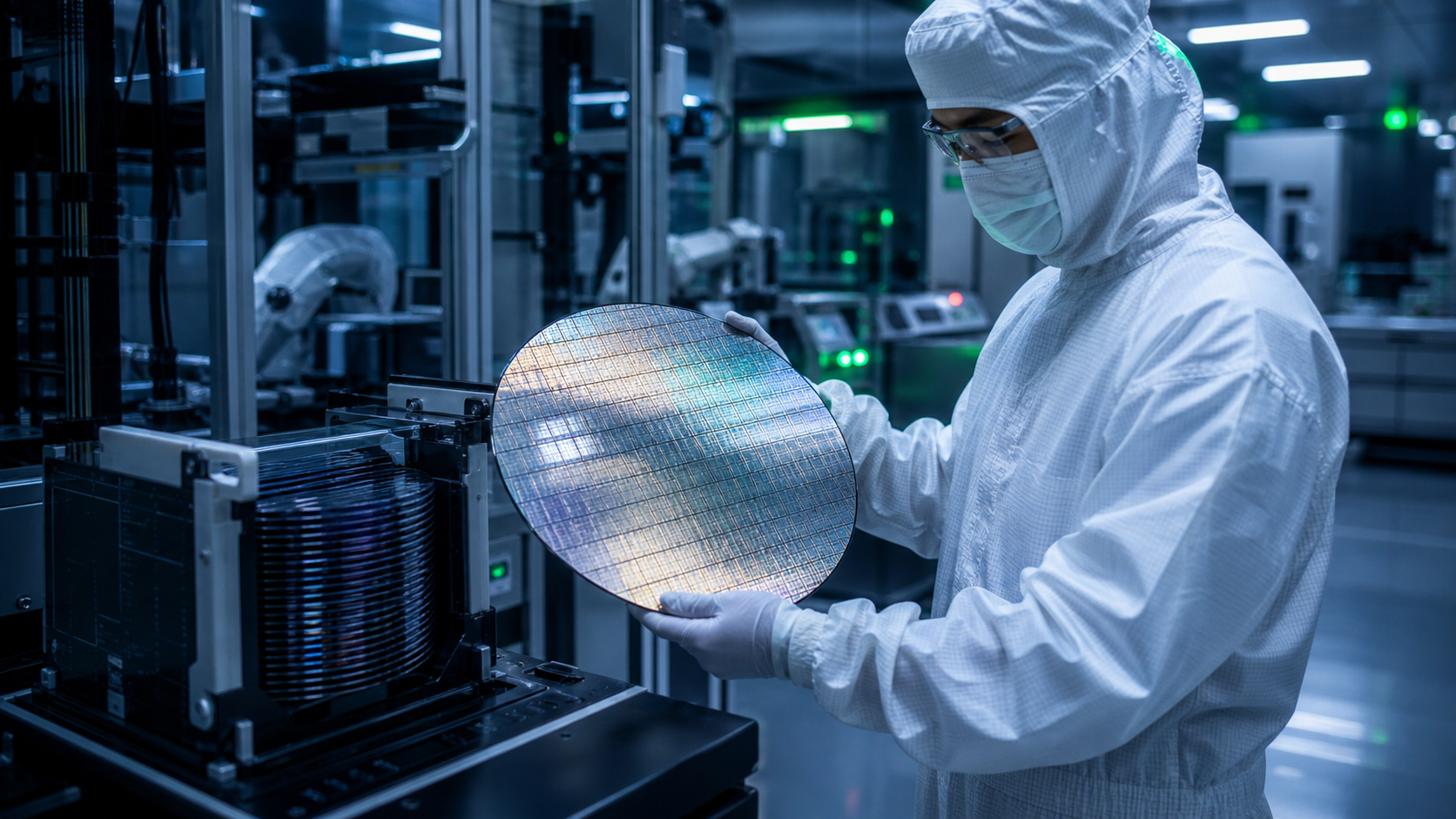
- Maia 300 separates compute chiplets fabricated on TSMC N2P from memory-controller and I/O functions on other dies.
- Each accelerator is specified with eight HBM4 stacks, 288GB of memory and a peak bandwidth of 18TB/s within a 950W TDP.
- Microsoft plans 96 accelerators across 24 trays in a 167kW rack and says production deployments will begin in 2027.
Microsoft has described the compute, memory and networking architecture of Azure Maia 300, its forthcoming accelerator for large-scale AI inference. The design puts compute chiplets manufactured using TSMC’s N2P process alongside separate memory-controller and input/output dies, with the system intended to enter production deployments in 2027. Maia 200 is already operating on Microsoft workloads; the new generation’s performance claims concern hardware that has yet to complete an equivalent production rollout.
AI inference can spend substantial time moving information rather than performing arithmetic. Large language models repeatedly transfer weights, intermediate results and attention state between processing units and memory, especially when producing long responses or serving many sessions concurrently. Adding arithmetic capability alone will not necessarily improve throughput when compute engines cannot obtain the required data quickly enough. Microsoft has consequently developed Maia 300 as a combined silicon, software and rack platform, rather than specifying the processor independently of its interconnect.
The chiplet arrangement places performance-sensitive compute on N2P while separating functions concerned with memory and external communication. That partition allows the different dies to be designed for their respective tasks, but requires close control of the connections and communication between them. The contribution of each design choice to workload performance remains difficult to separate because the process technology, packaging and memory subsystem operate together.
Each Maia 300 accelerator is specified with eight HBM4 stacks delivering 288GB of capacity and up to 18TB/s of peak memory bandwidth, within a 950W thermal design power. HBM places stacks of memory close to compute silicon through advanced packaging, providing a wide data interface and reducing the distance travelled by signals. Peak bandwidth is an interface specification, however, and does not imply that software can sustain the maximum rate with every model, access pattern or degree of memory contention.
Microsoft is also moving away from a uniform on-chip memory model towards a non-uniform arrangement that makes data locality explicit. Its software-defined dataflow architecture coordinates direct memory access engines, on-die SRAM, HBM and the on-chip network, enabling software to place frequently used information near the compute engines that require it. The approach can avoid some repeated transfers, but makes efficient scheduling and memory-aware programming important parts of achieving the proposed gains.
Enhanced MXFP4 support and selected storage formats using fewer than three bits further reduce the amount of information that needs to be moved or held during inference. Narrow representations may increase the effective capacity available to a model, though their suitability depends on scaling, conversion and a workload’s tolerance for numerical error. Microsoft has also described changes to vector instructions for softmax and data conversion. These are disclosed design features, rather than evidence that all models retain their accuracy without retraining or calibration.
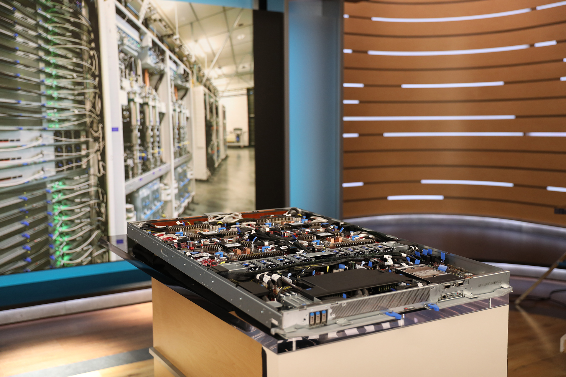
At rack level, the company plans 96 accelerators in 24 trays of four, within a 167kW electrical envelope. Microsoft specifies 27.6TB of combined HBM capacity and an aggregate peak bandwidth of around 1.7PB/s for that configuration. The totals add together memory resources distributed across numerous devices: software cannot assume that memory on another accelerator has the same access time as local HBM. Each tray also contains host processing, storage and cooling resources, while shared switching and power equipment form part of the rack design.
A two-tier scale-up network extends communication beyond a single rack. Direct electrical links and switched connections join accelerators within a rack, while optical links connect racks through a second switching tier. Microsoft describes a scale-up domain reaching 12,288 accelerators, with custom transport using Ethernet-based infrastructure. Such connections are necessary when a model is partitioned across devices, but latency, synchronisation and network occupancy still determine how much of the aggregate hardware a particular inference job can use.
With 96 accelerators operating in a rack rated at 167kW, the power and cooling architecture has to support tightly packed hardware. Microsoft specifies dual feeds, a 50V busbar distribution system and liquid cooling that removes more than 80% of rack thermal load, with air cooling for ancillary equipment. Those arrangements must be engineered around the facility’s electrical and water infrastructure. The 167kW rack envelope is not equivalent to the full data centre power requirement, which also includes cooling plant and other facility loads.
Microsoft projects up to seven times the rack-scale token throughput of Maia 200 and more than 2.5 times the performance per watt, with the comparisons reflecting differences in accelerator count and system architecture as well as chip characteristics. These remain manufacturer estimates rather than independently reproduced application benchmarks. Maia 300’s first production deployments are planned for 2027, when sustained operating data may provide a firmer basis for comparison.