IN Brief:
- The proposed board delivers 24kW in a 400 × 60mm form factor for NVIDIA MGX compute trays.
- Sixteen 650V GaN transistors use a stacked half-bridge topology on the primary side.
- The 97% full-load efficiency figure is a design target, with no independent qualification results disclosed.
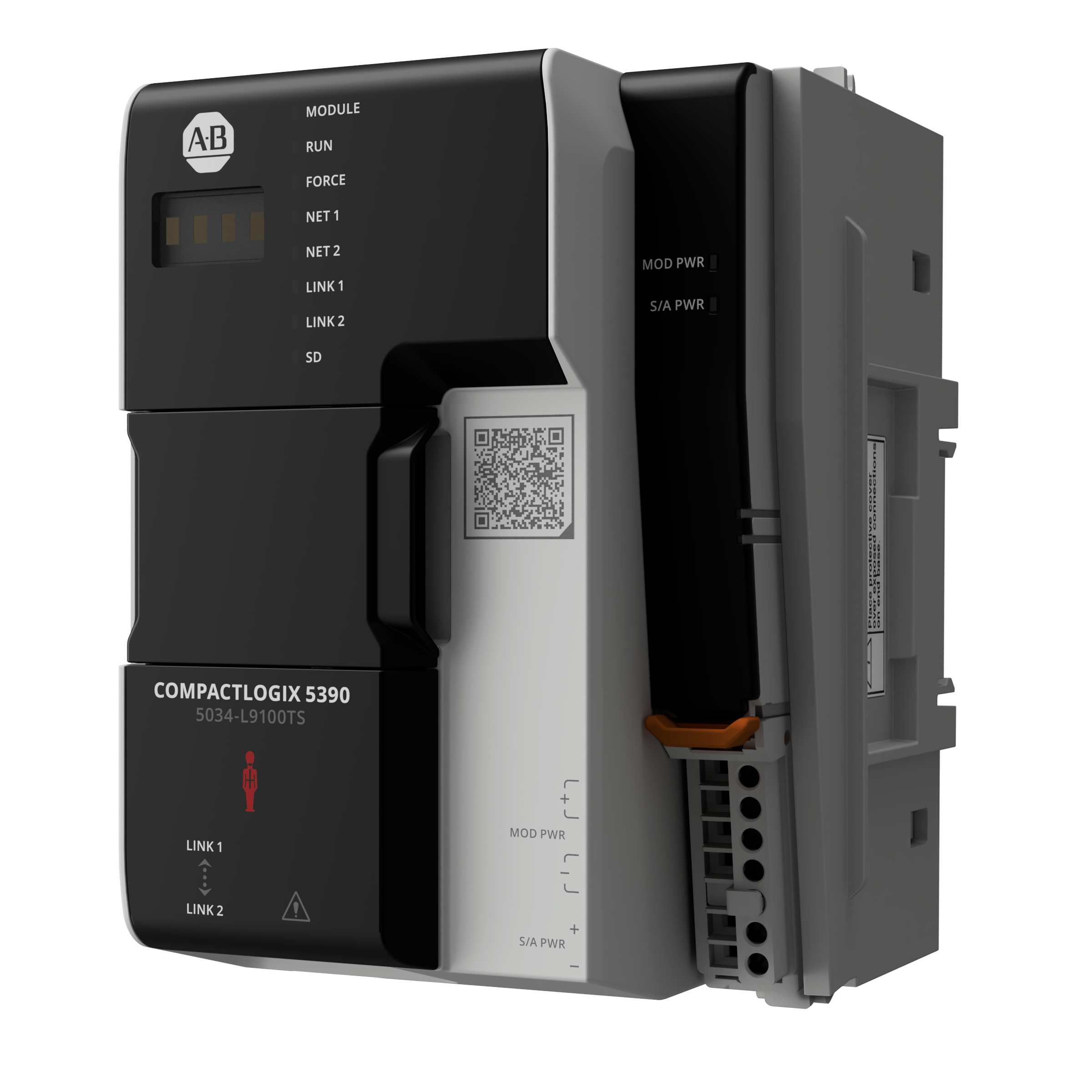
Navitas Semiconductor has developed a 24kW DC-to-DC power delivery board that converts an 800V data centre distribution supply directly to 12V for accelerator compute trays. Designed with NVIDIA for its MGX ecosystem, the GaN-based assembly is intended to sit close to processing hardware and replace an intermediate conversion stage used in alternative rack power architectures. Navitas plans to display the board at the Open Compute Project Global Summit in October 2026.
The new design follows a previously announced 20kW board converting 800V to 6V, described in earlier coverage of Navitas power conversion development. Both developments concern the distribution of increasingly high electrical power to AI computing equipment, but they use different output voltages and power ratings. The latest board is a separate hardware design, rather than a revision of the earlier board’s stated 6V output.
An 800V DC distribution bus can transport a given amount of power at a lower current than a low-voltage bus, reducing current-related losses over the upstream wiring. At the compute tray, however, the supply must be stepped down substantially before it reaches a processor voltage regulator. One approach converts 800V through an intermediate bus, such as 50V, and then down to 12V. Navitas says its new board removes the intermediate 50V-to-12V converter by carrying out the 800V-to-12V conversion in one stage.
The 12V output still feeds a voltage regulator module, which performs the final conversion to the much lower operating voltages required by accelerator silicon. Eliminating the intermediate stage therefore does not remove point-of-load regulation. It changes the partition of the power system, transferring more of the voltage reduction into a compact converter next to the compute hardware. Higher current on the 12V side makes conductor resistance, connector design and physical proximity to the voltage regulator particularly important.
Navitas specifies sixteen NV6034 GaNFast field-effect transistors rated at 650V and 18mΩ on the primary side, arranged in a stacked half-bridge topology. The devices use dual-cooled DFN 8 × 8 packages. Stacking switches allows a design to distribute voltage stress across devices, but the arrangement also requires control of switching transitions, voltage sharing and fault behaviour. Device voltage ratings cannot simply be added together without accounting for transient conditions and the supporting circuit.
The board is designed around a 400 × 60mm NVIDIA form factor, with a target power density above 2,000W per cubic inch and an efficiency target of 97% at full 24kW load. These are manufacturer-specified design objectives, not independently verified results from a deployed data centre. Achieving high power density also concentrates thermal loads, making heat extraction through packages, the board and its cooling interface part of the converter’s engineering performance.
Fast-switching GaN devices can reduce switching losses under suitable conditions, while their high edge rates place demanding requirements on parasitic inductance, gate-drive timing and electromagnetic compatibility. The stacked primary-side topology introduces further coordination requirements between semiconductor switches. Input protection, isolation arrangements where required by the final architecture, and behaviour during load changes must be established at system level rather than inferred from the semiconductor specification.
Placing the converter on or close to the compute motherboard could shorten some low-voltage current paths and simplify the arrangement of separate intermediate-bus hardware. The outcome will depend on the specific tray layout and how its cooling, service access and protection zones are arranged. Navitas has not disclosed a complete loss breakdown against a named alternative architecture, so an improvement in board-stage efficiency should not be treated as a measured improvement for an entire rack.
Navitas intends to demonstrate the 24kW board within NVIDIA’s MGX ecosystem at the October summit. The company has not supplied measured efficiency curves, thermal qualification results or deployment volumes for the design, so comparison with intermediate-voltage architectures remains limited to its stated targets and converter arrangement.