IN Brief:
- Siemens is demonstrating virtual AOI preparation at its electronics factory in Erlangen.
- Teamcenter, Process Preparation X, and NVIDIA Cosmos generate board representations and synthetic inspection images.
- Targets include up to 85% less manual AOI programming work and more than 40% fewer false calls.
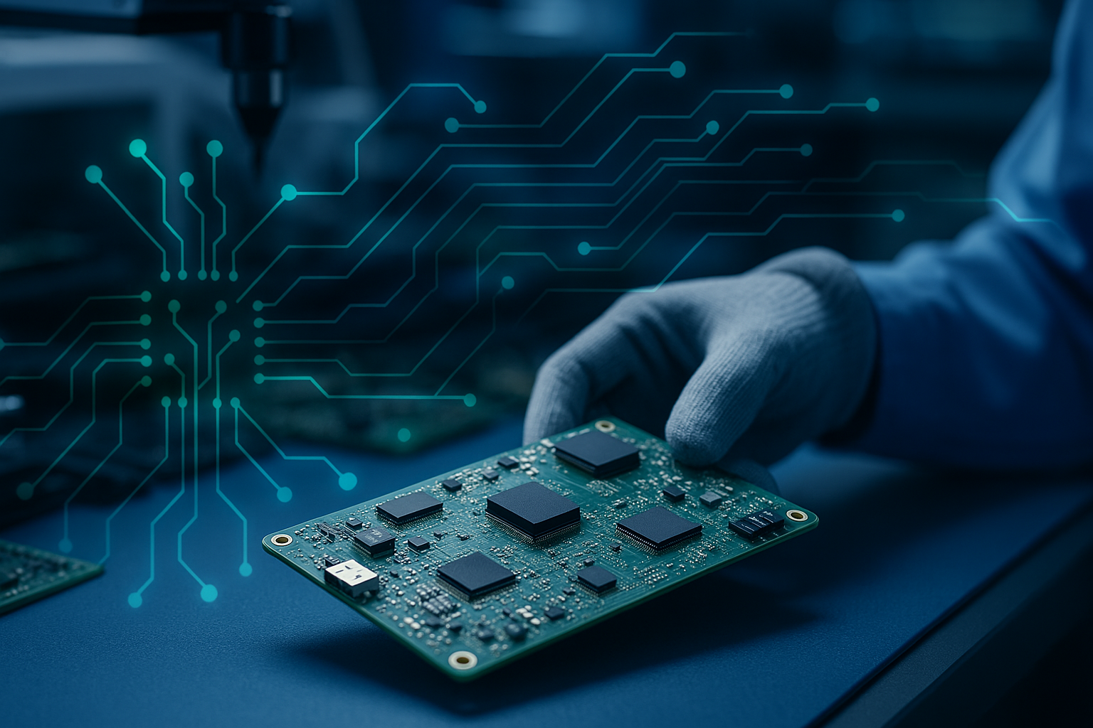
Siemens and NVIDIA are developing a virtual preparation workflow for automated optical inspection of printed circuit board assemblies, aiming to configure inspection processes before the first physical production board is available.
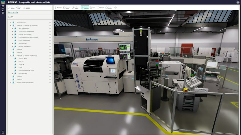
The collaboration combines Siemens Teamcenter and Process Preparation X with NVIDIA Cosmos to create digital representations of assembled boards and generate synthetic images for inspection preparation. Siemens is demonstrating the approach at its electronics factory in Erlangen, Germany, where the production environment accommodates frequent product changes and places considerable demands on manufacturing preparation.
Automated optical inspection, or AOI, checks assembled circuit boards for visible manufacturing defects and component placement problems. A system may identify a suspicious solder joint, incorrectly oriented device, missing component, or other departure from the expected assembly. Its usefulness depends on the inspection programme recognising actual defects without overwhelming operators with indications that prove acceptable on review.
Preparing that programme has traditionally depended on obtaining representative physical boards. Engineers establish reference images, set inspection parameters, and examine how the equipment responds to components, solder features, and normal variations in appearance. These steps take time when a factory introduces a new assembly or changes a component, even where the electronic design itself is ready for manufacture.
Teamcenter supplies the PCB design, bill of materials, and component information needed to describe the intended assembly. Process Preparation X validates and normalises those inputs, then assembles them into a digital twin of the printed circuit board assembly. This information provides the starting point for generating a reference board without relying entirely on a built prototype.
The virtual reference, sometimes called a golden board, represents the intended correct assembly. NVIDIA Cosmos is used to create photorealistic images of that representation and synthetic images showing defects or other conditions that inspection equipment might encounter. The resulting data can support the calibration and preparation of AOI programmes before a physical board reaches the line.
Producing usable images requires more than a geometrically correct board model. Component finishes, solder surfaces, illumination, viewing angles, and the characteristics of the inspection camera can influence the appearance of a feature. A virtual image that fails to represent those conditions could train the system to accept an actual defect or incorrectly reject a satisfactory assembly.
Siemens is therefore connecting engineering data with image generation and subsequent inspection analysis rather than treating synthetic data as a substitute for all physical verification. The workflow extends into manufacturing through an AI-supported secondary inspection step. When the AOI system flags a possible fault, this additional analysis helps determine whether the finding is genuine or a false call.
False calls can interrupt production because operators must investigate boards that may be fully functional. Repeated review also occupies inspection equipment and manufacturing personnel, especially where a facility handles many designs in relatively small batches. Reducing those interruptions would be useful only if defect detection remains sufficiently sensitive for the applicable manufacturing quality requirements.
At Erlangen, Siemens is targeting up to 85% less manual engineering effort in generating AOI programmes. The project also targets more than 40% fewer false calls and a first-pass yield improvement exceeding 5%. These are stated objectives, not measured outcomes from a completed production validation. Siemens has not provided independently audited results or a comparison across different inspection equipment manufacturers.
The choice of Erlangen reflects the factory’s changing product mix. Siemens says the site can introduce changes three to five times a week, creating repeated demand for programme preparation, operator assessment, and line readiness. Preparing an inspection recipe earlier could reduce the interval between an engineering revision and its introduction to manufacturing, provided that the virtual models are kept aligned with current design data.
A design revision can alter component position, package geometry, or the expected solder appearance, so inspection preparation cannot remain isolated from the source design. Connecting it to product lifecycle information creates a route for propagating changes into manufacturing software, while actual boards continue to provide evidence that the resulting programme performs correctly.
The companies have not given a general commercial availability date or detailed performance results for different PCB types. The Erlangen demonstration will provide a practical setting in which to establish how well digitally prepared inspection programmes handle real component variation, physical defects, and the pace of electronics production changes.