IN Brief:
- SETT has issued three preliminary market consultations for 30 of the 60 planned semiconductor research tools.
- A 2,000m² cleanroom is planned for 300mm process research and prototyping, not announced volume chip production.
- Supplier responses for the latest ten-tool exercise are due by 15 March 2027; no equipment award has been made.
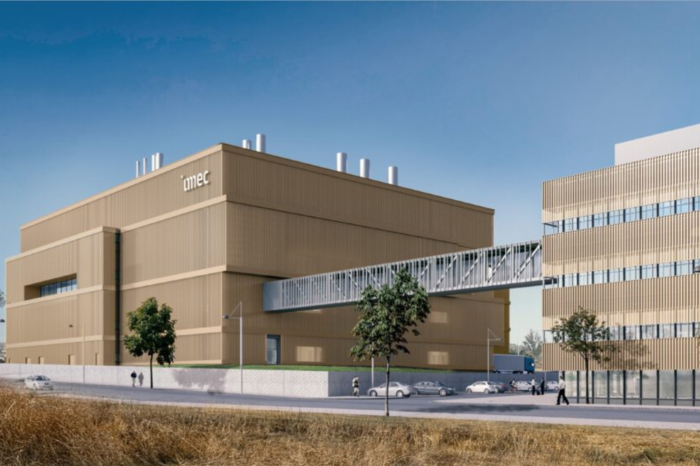
Spain’s Sociedad Española para la Transformación Tecnológica (SETT) has opened preliminary market consultations for equipment at the planned imec research centre in Málaga. Three consultations now cover 30 of the 60 specialised tools intended for its cleanroom, including a ten-machine exercise published on 13 November. Construction of the centre is planned to start in the first quarter of 2027.
The latest consultation invites potential suppliers to describe technical options, expected delivery periods, and indicative costs, with responses due by 15 March 2027. This is market engagement before formal procurement, not a tender award or confirmation that any particular manufacturer will provide equipment. Final specifications and supply contracts have yet to be determined.
The centre is planned for Málaga TechPark and will include a 2,000-square-metre cleanroom dedicated to research and prototyping on 300mm wafers. SETT has put the expected investment in advanced processing equipment at €267 million, including €150 million from funds managed through its programme. The Spanish central government has committed €500 million to the wider project, with additional support from the Andalusian regional government.
The most recent ten-tool exercise spans deposition, patterning, removal, and inspection. Reported equipment categories include chemical mechanical planarisation, physical vapour deposition, metal etching, a photolithography track, X-ray fluorescence analysis, optical inspection, electron-beam review, scanning acoustic microscopy, overlay measurement, and tape mounting. These describe the types of capability under consultation, not final machine selections or completed purchase orders.
Each operation fits into a distinct part of wafer processing. Physical vapour deposition lays down thin films, etching removes selected material, and chemical mechanical planarisation smooths topography for subsequent layers. A photolithography track handles the coating and treatment steps associated with pattern transfer; the ultimate resolution also depends on separate exposure equipment and process conditions, which the current consultation does not establish.
Metrology and inspection determine whether those processes have achieved the intended geometry and material characteristics. Optical overlay measurements assess alignment between patterned layers; electron-beam review can examine small defects or structures at higher spatial resolution; and scanning acoustic microscopy can detect some internal defects or interfaces without destroying the specimen. The final measurement capability will depend on the instruments specified and their performance limits.
The new centre is intended to provide an experimental research platform rather than the output volumes of a commercial foundry. Its 300mm equipment would allow researchers to investigate processes and materials on the wafer diameter widely used by advanced semiconductor manufacturers. Demonstrating that a process works on that substrate size can improve the relevance of subsequent transfer discussions, although pilot-line results do not themselves prove manufacturability at industrial yields and volumes.
The Málaga site is intended to complement imec’s advanced CMOS research facilities at Leuven in Belgium. Its work is expected to involve new materials and processes that can be explored on industry-standard wafer sizes. Exactly which research processes will be divided between Málaga and Leuven will depend on available equipment, project selection, contamination requirements, and the integration of experimental materials into the process flow.
Installing a processing line requires more than completed cleanroom floorspace. Semiconductor processing equipment needs tightly managed environmental conditions, stable utilities, contamination controls, and services appropriate to individual chemical, vacuum, electrical, and thermal processes. A tool may be mechanically installed but still require facility connections, safety checks, process qualification, and calibration before it can contribute to research output.
Earlier in 2026, the construction contract was awarded and the Spanish government set a first-quarter 2027 start for building works. The building phase is expected to continue into 2028; reporting has indicated an intended operating horizon around 2030, but that remains a planning expectation, not an independently established commissioning date. Installation and qualification of the process tools will follow their procurement and delivery schedules.
SETT’s September project outline estimated approximately 200 direct skilled jobs and 500 indirect jobs in Málaga and its province, with additional employment elsewhere in Spain. Those are projections associated with an unfinished facility. The procurement programme nevertheless creates a more immediate test of the project’s schedule, because long-lead semiconductor tools must be specified and ordered sufficiently early to support the intended commissioning sequence.
SETT must first convert supplier responses into equipment specifications and formal tenders. Those decisions will determine the configuration, interfaces, and delivery sequence of a research line whose individual tools must work together. Until suppliers are chosen and instruments commissioned, the centre’s 300mm capability remains planned rather than available for research users.