IN Brief:
- Twenty-one State aid decisions support semiconductor projects representing more than €33bn in combined public and private investment.
- The latest approvals include €57.6m in German support for wafer dicing equipment and semiconductor precursor materials.
- The figures describe investment associated with approved projects, not completed expenditure or a new €33bn funding allocation.
The European Commission has approved 21 State aid decisions supporting first-of-a-kind semiconductor facilities, with the associated projects representing more than €33bn in combined public and private investment across the European Union.
The milestone, detailed on 17 November, covers activities throughout the semiconductor supply chain, including wafer manufacturing, advanced packaging, testing, assembly, specialist materials, production equipment, and power electronics.
The €33bn figure represents investment associated with the approved projects rather than a new allocation of European public funding. It combines public and private capital and does not establish that all the facilities have been constructed or that the full amount has already been spent.
The decisions fall under the second pillar of the European Chips Act, which addresses security of supply and industrial resilience. The framework seeks to increase semiconductor production capabilities within Europe while supporting development of the wider manufacturing ecosystem.
Its first-of-a-kind approach concerns facilities introducing manufacturing capabilities that are not already substantially present within the European Union. Such projects may involve specialised production processes or manufacturing technologies that expand the range of semiconductor activities available in the region.
State aid approval is necessary because national subsidies are subject to European competition rules. Public authorities must establish that proposed support is appropriate and proportionate, rather than providing unlimited financial assistance to industrial projects.
The Commission examines whether the measures can facilitate economic activity while avoiding undue distortion of competition and trade between Member States.
The latest milestone follows two German aid approvals announced on 16 November, with a combined budget of €57.6m. These were the twentieth and twenty-first decisions assessed using the principles of the European Chips Act Communication.
The first measure provides €43.5m in support for Lidrotec, which plans to establish a facility in Bochum producing laser-based equipment for semiconductor wafer dicing.
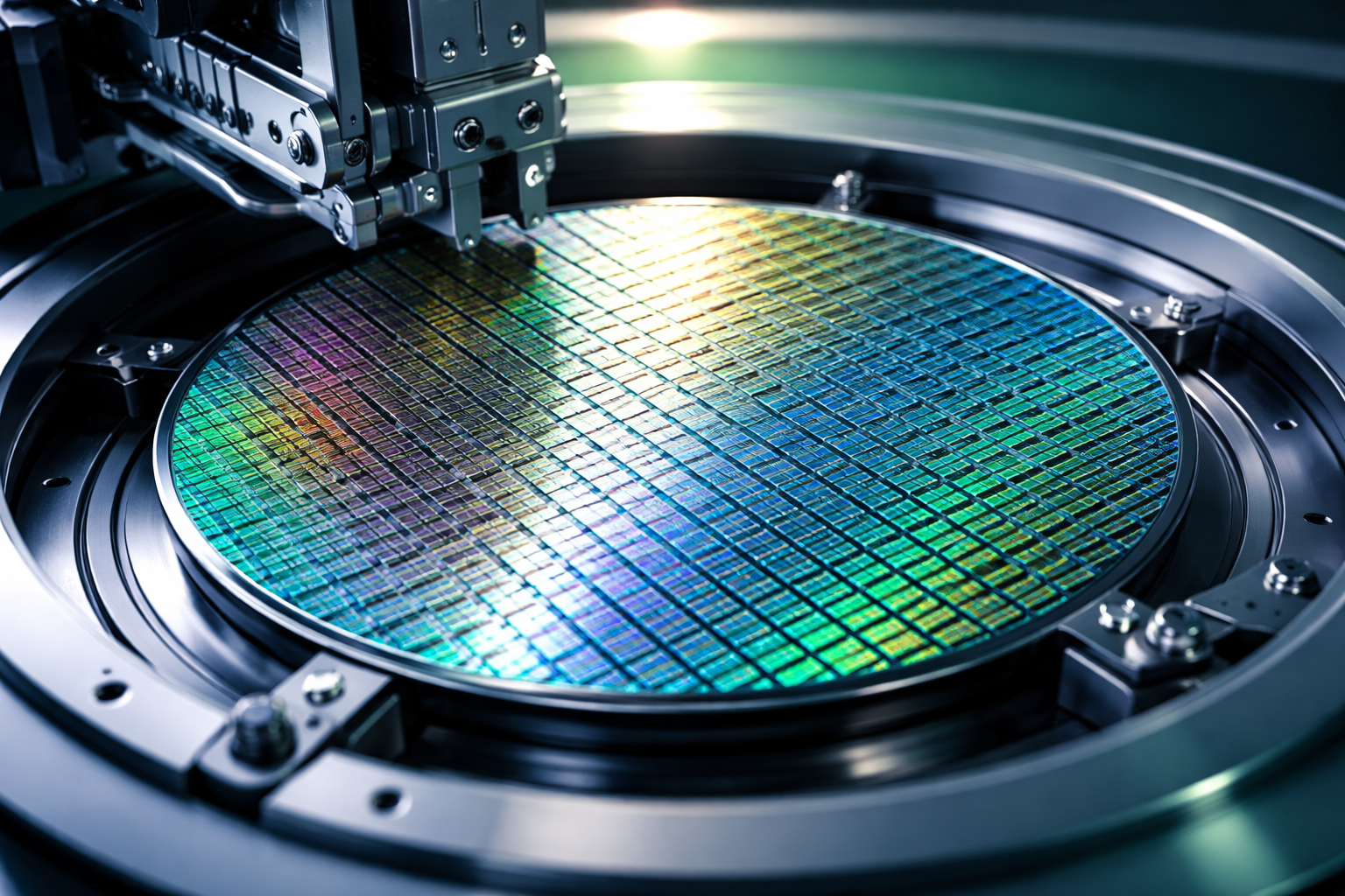
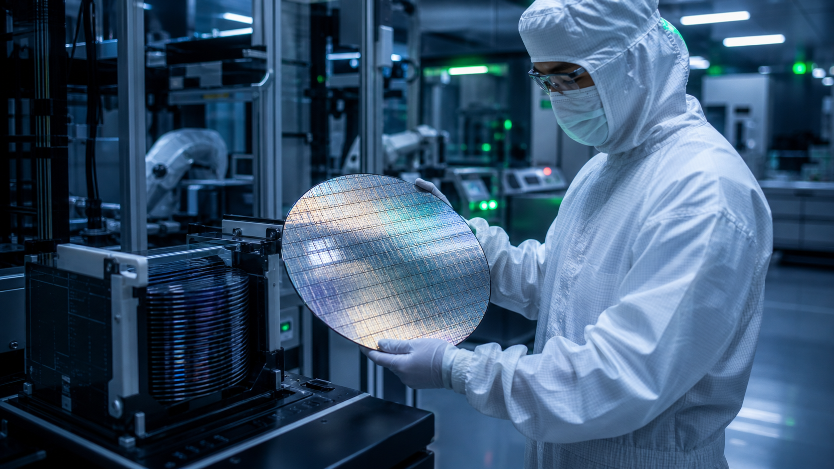
Dicing separates the individual semiconductor devices formed on a wafer after the relevant manufacturing processes have been completed. The operation must produce accurate cuts while limiting damage to the semiconductor structures and maintaining suitable manufacturing throughput.
Conventional separation processes can involve mechanical cutting, while laser-based approaches use concentrated optical energy to remove material or produce the conditions required for separation.
Different technologies present trade-offs involving processing speed, cut width, material compatibility, mechanical stress, and thermal effects. The selected method must be appropriate for the wafer material, device construction, and subsequent packaging requirements.
Lidrotec’s project concerns the production of semiconductor manufacturing equipment rather than the construction of a new wafer fabrication plant.
Equipment manufacturing is nevertheless an important part of semiconductor supply capacity. Fabrication facilities depend on specialist tools for multiple stages of production, and delays in obtaining or qualifying those tools can affect the introduction of additional manufacturing lines.
The second German measure provides €14.1m for Dockweiler to establish production of critical precursor chemicals used in semiconductor manufacturing.
These materials contribute to processes that require tightly controlled chemical composition, purity, and contamination levels. Their properties can influence the repeatability of manufacturing operations and the quality of the resulting semiconductor structures.
Establishing additional regional production capacity may provide alternative sources of materials, but semiconductor manufacturers must still qualify suppliers and confirm that the resulting products satisfy their established process requirements.
Changes to a material supply route can require testing because apparently small variations in composition or impurities may affect production behaviour.
The two projects address different points in the same manufacturing ecosystem. One concerns equipment used during wafer separation, while the other provides inputs to semiconductor fabrication processes.
Their approval demonstrates that investment in semiconductor capacity extends beyond the construction of advanced logic fabs. Materials, equipment, assembly, packaging, and testing are also necessary to deliver completed components.
Earlier decisions assessed under the same approach accounted for approximately €15.2bn in approved national State aid. That public support figure differs from the more than €33bn in combined public and private investment associated with the wider portfolio.
The distinction is important when evaluating expenditure. Approved public support is not identical to private capital committed by companies, and neither measure should automatically be interpreted as completed investment.
Europe’s semiconductor requirements are also technologically diverse. Automotive electronics, industrial control systems, communications hardware, medical devices, and computing infrastructure use different semiconductor processes and component architectures.
Advanced computing processors may depend on leading-edge manufacturing and complex packaging, while industrial equipment can require power devices, analogue components, sensors, and controllers produced using other process technologies.
A broader manufacturing base therefore requires investment in several types of equipment and facilities rather than concentrating solely on the smallest available transistor geometries.
The Commission’s approved projects cover a range of those capabilities. Their eventual contribution to regional supply will depend on construction, production qualification, operating costs, manufacturing yields, and customer demand.
New facilities must also secure specialist personnel, reliable equipment, materials, and supporting infrastructure. State aid approval can enable a project to proceed, but it cannot eliminate those manufacturing and commercial constraints.
The European Chips Act also includes research and pilot manufacturing activities intended to support semiconductor development. These operate alongside the State aid framework, with different mechanisms and objectives.
The Commission’s latest milestone establishes the scale of projects approved under its industrial support approach. Their impact on semiconductor availability will become measurable as facilities enter production, achieve the necessary qualifications, and begin supplying commercial customers.