IN Brief:
- SiTime has launched FemtoClock 4 and VersaClock 8 for high-speed networking and computing platforms.
- FemtoClock 4 provides up to 18 outputs and manufacturer-specified 19fs RMS phase jitter under defined measurement conditions.
- VersaClock 8 targets PCIe 7 clocking, with five-, nine-, and twelve-output variants operating at temperatures up to 105°C.
SiTime Corporation has introduced FemtoClock 4 and VersaClock 8, two programmable clock families designed for the higher data rates required by AI servers, Ethernet switches, and computing infrastructure. The devices address timing requirements associated with 224G serializer-deserializer links and PCI Express 7 interfaces, combining low phase jitter with multiple clock outputs and compact packaging.
FemtoClock 4 primarily targets Ethernet switching equipment, including top-of-rack and spine switches using high-speed SerDes connections. VersaClock 8 provides programmable reference clocks for processors, accelerators, storage interfaces, and other computing components, with particular emphasis on the timing requirements of PCIe 7.
Both families extend technologies acquired through SiTime’s purchase of Renesas’ timing business in July 2026. FemtoClock and VersaClock were established product families before that transaction, while the new generations introduce configurations intended for the faster interconnects being developed for high-density computing systems.
As serial data rates increase, the quality of reference timing becomes an increasingly important electrical design constraint. A serializer-deserializer converts information between parallel and serial data formats, allowing large amounts of information to move over high-speed connections between integrated circuits.
The transmitting and receiving devices must operate with sufficiently accurate timing to recover the data reliably. Variations in clock timing, known as jitter, reduce the margin available for distinguishing individual data symbols and can contribute to transmission errors.
The acceptable amount of jitter depends on the interface specification, operating frequency, measurement bandwidth, and characteristics of the complete signal path. Clock performance figures must therefore be interpreted under their stated test conditions rather than compared without regard to how they were measured.
SiTime identifies progressively tighter reference clock requirements as Ethernet SerDes links move towards 224G operation. Its technical guidance describes typical jitter allowances falling from below 150 femtoseconds for 56G interfaces to below 35 femtoseconds for 224G designs.
FemtoClock 4 is specified to deliver 19 femtoseconds RMS phase jitter at 312.5MHz in clock generator mode. The figure applies over a measurement range of 12kHz to 20MHz using a 4MHz high-pass filter, and should not be interpreted as a universal jitter value for every operating mode or frequency.
The family provides up to six independent frequency domains across eighteen clock outputs. This allows different parts of a network switching system to receive suitable reference frequencies from a consolidated clock generation architecture.
High-density switches can require numerous reference clocks for their SerDes interfaces, processors, and peripheral circuitry. Consolidating outputs can reduce the number of separate clock generators required, although the arrangement still depends on PCB routing, power supply noise, output loading, and other electrical constraints.
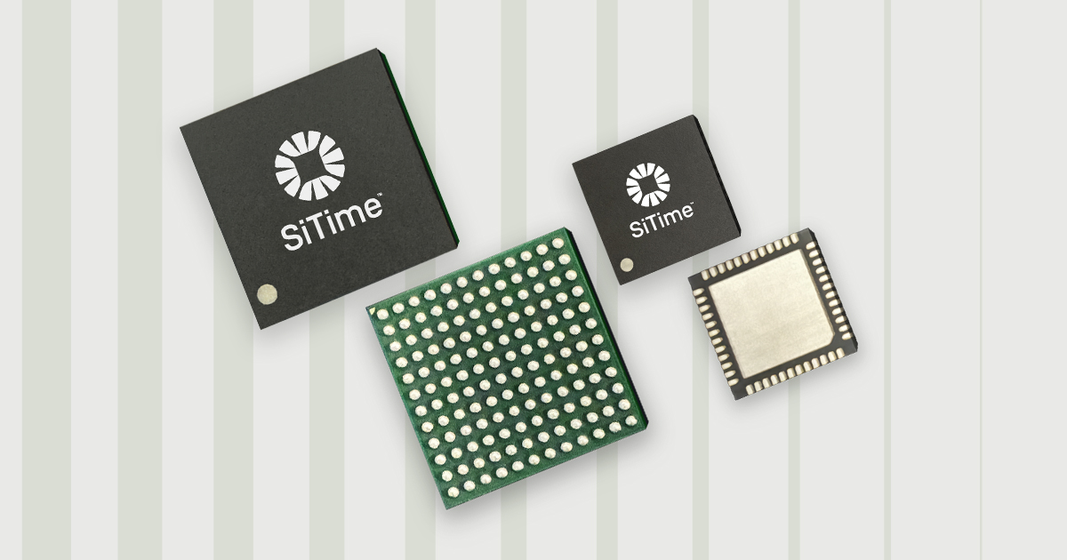
FemtoClock 4 offers twelve outputs in a 9 × 9mm BGA package or eighteen outputs in a 10 × 10mm BGA package. The configurations allow designers to select a balance between the number of clock connections and the board area available for the timing hardware.
VersaClock 8 addresses the separate requirements of internal computing interfaces. PCIe 7 is designed to double the data transfer rate of PCIe 6, increasing the importance of reference timing as faster signals move between processors and connected devices.
SiTime specifies approximately 10 femtoseconds of reference clock jitter for PCIe 7 applications, alongside a 30-femtosecond RMS phase jitter figure at 312.5MHz under its stated integration and filtering conditions. These figures describe different timing measurements and should not be treated as interchangeable specifications.
The family offers five-, nine-, and twelve-output configurations in QFN packages ranging from 4 × 4mm to 6 × 6mm. SiTime states that its twelve-output version occupies approximately 40% less board area than a comparable solution, although the comparison is dependent on the chosen reference design.
VersaClock 8 also supports operation at temperatures up to 105°C. This is relevant to computing boards containing densely installed processors, memory, and high-speed interfaces, where local temperatures can be elevated by the heat dissipated across the assembly.
The clock generator’s own electrical power consumption influences its contribution to local heating. SiTime identifies low power consumption as a feature of VersaClock 8, but actual thermal performance will depend on the selected device, clock configuration, output loading, and operating conditions.
Both product families can be incorporated into one system. A top-of-rack switch might use FemtoClock 4 to generate clocks for its Ethernet SerDes interfaces while employing VersaClock 8 for the processor and PCIe connections.
This division reflects the different reference frequencies, output requirements, and jitter budgets associated with network-facing interfaces and internal computing connections. The complete clock tree must also account for power sequencing, distribution losses, and any required synchronisation between system functions.
SiTime estimates that FemtoClock 4 and VersaClock 8 address a serviceable market worth approximately $2 billion over five years. That is the company’s assessment of a potential market opportunity, rather than a confirmed order value or revenue commitment.
Both clock families are in production and available. Their introduction gives system designers additional component options for 224G Ethernet and PCIe 7 hardware, with suitability determined by the required frequency domains, output count, jitter specifications, package constraints, and operating environment.