IN Brief:
- iPHEMOS-DDX can dock directly to semiconductor testers from three directions for analysis under operating conditions.
- Seven integrated analytical techniques cover optical emission, thermal, laser and electro-optical failure localisation.
- Orders opened globally on 29 September, with the system due to appear at ISTFA 2026 in Texas during October.
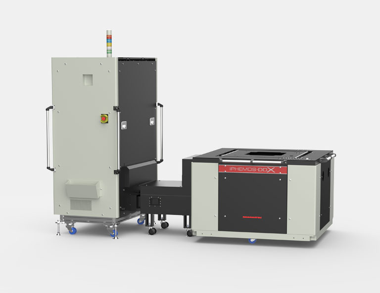
Hamamatsu Photonics has launched the iPHEMOS-DDX inverted emission microscope for failure analysis of advanced semiconductor packages, targeting devices built around chiplets, High Bandwidth Memory and 2.5D or 3D integration.
The system can dock directly to semiconductor testers from three directions, allowing it to be installed around an existing tester-based measurement environment. Hamamatsu has also combined seven analytical techniques in one platform so several stages of electrical failure localisation can be carried out without repeatedly transferring a device between separate instruments.
Direct tester access is increasingly relevant as semiconductor packages become more integrated. Some failures only appear while the device is executing a particular pattern or operating under high speed electrical conditions, making static inspection insufficient to reproduce the fault.
Keeping the package connected to the tester allows electrical stimulus and physical localisation to take place in the same setup. The arrangement reduces the risk that a difficult intermittent condition disappears when the sample is disconnected, moved and reinstalled on another piece of analysis equipment.
The seven techniques include photon emission microscopy, thermal and lock-in thermography methods, laser scanning microscopy, OBIRCH, DALS, EOP or EOFM and time dependent imaging. They use different optical, thermal and electro-optical effects to identify abnormal activity inside a device or package.
No single method covers every failure mechanism. Photon emission can reveal light generated by abnormal current flow, thermal techniques can expose local heating, while laser-based approaches can perturb or probe electrical behaviour. Electro-optical methods add information on dynamic activity that may be difficult to infer from a static image.
Combining these functions becomes more useful as physical access to the active silicon deteriorates. A modern accelerator package can contain large logic dies, multiple HBM stacks, interposers and several layers of interconnect, creating a much more complicated structure than a conventional single-die package.
The package dimensions also increase the mechanical demands on the analysis system. The microscope has to move across a comparatively large assembly while retaining sufficient positional stability to correlate electrical behaviour with a local structure. Thermal drift and vibration can become significant when measurements have to remain aligned over long acquisitions.
Advanced packaging also changes the possible location of the failure. A defective system may contain a fault in the logic die, memory stack, interposer, package routing or interface between those elements. Failure localisation consequently has to narrow the problem before destructive analysis begins, particularly when the package contains several expensive devices.
The tester itself is another practical constraint. Production and development laboratories can be organised around large automatic test systems that are difficult to reposition, so analysis equipment that only docks from one direction can create an installation problem before a measurement begins.
Hamamatsu’s three-direction docking arrangement gives laboratories more flexibility over how the microscope is positioned relative to existing equipment. The mechanical feature is mundane compared with the optical techniques inside the instrument, but it affects whether the system can be incorporated into a working failure-analysis environment without rebuilding the tester layout.
The consolidated workflow can also reduce repeated sample handling. Moving an advanced package between instruments introduces setup time and can alter cabling, thermal conditions or test configuration. Keeping several techniques around the same tester connection preserves more of the measurement state between analytical steps.
Hamamatsu opened worldwide orders for iPHEMOS-DDX on 29 September. The company is targeting semiconductor manufacturers and semiconductor equipment suppliers and will exhibit the system at ISTFA 2026 in Texas from 4 to 8 October.
The instrument arrives as packaging complexity is increasing faster than simple optical access can accommodate. Chiplets and stacked memory allow more functionality to be assembled inside one package, but every additional die and interface creates another possible failure location.
iPHEMOS-DDX addresses that problem by combining several localisation methods around a device that can remain electrically connected to its tester. Its value will ultimately be measured by how quickly a reproducible electrical failure can be narrowed to a physical location that design, packaging or process teams can investigate further.