
IN Brief:
- An eight-device silicon MOS spin-qubit array has been fabricated through a CMOS-compatible 300mm process.
- Coherent operation, shared readout, and an adjacent two-qubit gate were demonstrated across the linear array.
- Further scaling depends on device uniformity, automated calibration, cryogenic control, interconnect density, and repeatable foundry processes.
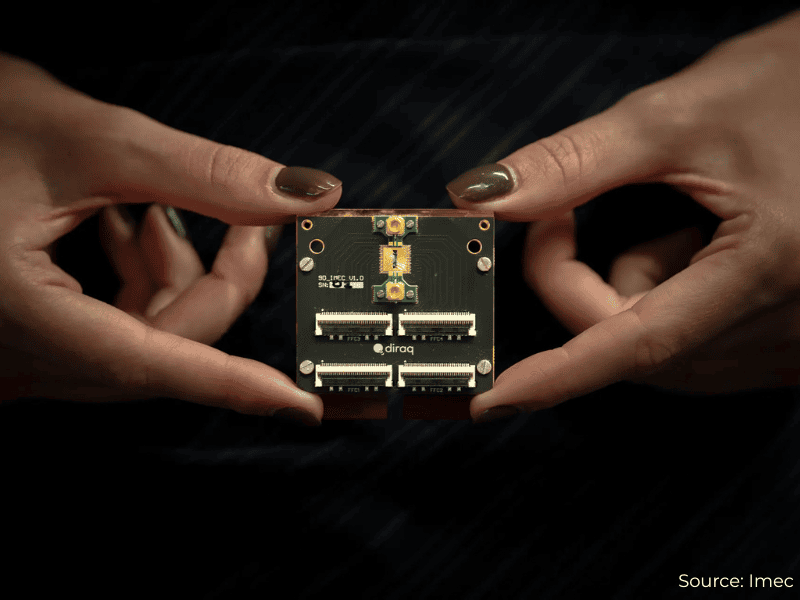
imec and Diraq have demonstrated coherent operation and readout across an eight-device silicon metal-oxide-semiconductor spin-qubit array fabricated through a CMOS-compatible 300mm process.
Designed by Diraq and manufactured on imec’s silicon spin-qubit platform, the linear array extends earlier work on individual devices and two-qubit building blocks into a structure containing four double quantum dots. Coherent control was maintained across the array rather than confined to a single selected pair.
Measurements included dephasing times reaching 41µs and Hahn-echo coherence extending to 1.31ms, while the partners also operated an adjacent two-qubit gate. A cascaded charge-sensing arrangement read the four central quantum dots without assigning a separate sensing chain to every qubit.
As arrays grow, the electronics surrounding each quantum device become a larger constraint. Dedicated sensors, control lines, and room-temperature instruments add wiring density and thermal load, while calibration becomes progressively harder to manage across devices whose operating points vary by small but consequential amounts.
By sharing readout resources, the cascaded architecture reduces the rate at which sensing hardware has to expand with qubit count. Multiplexing does not remove the need for accurate control, although it can ease pressure on the cryogenic interconnects and measurement chains that would otherwise dominate a larger processor.
Silicon spin qubits remain attractive partly because their materials and device structures have close parallels with conventional transistor production. A 300mm platform provides access to mature lithography, process monitoring, statistical metrology, and wafer-scale manufacturing methods that are difficult to reproduce in small research fabrication lines.
CMOS compatibility, however, does not make a spin-qubit device equivalent to ordinary logic. Quantum behaviour remains sensitive to interface roughness, material defects, charge noise, gate geometry, and small variations in electrostatic confinement, while the finished devices must operate at cryogenic temperatures far below those used by conventional integrated circuits.
The eight-device structure therefore provides a larger test of process uniformity as well as quantum control. Useful scaling will require a high proportion of quantum dots to tune into their intended operating windows, predictable coupling between neighbours, and calibration procedures capable of identifying and correcting variation without prolonged manual intervention.
Manufacturing programmes are beginning to address that transition. Imec is coordinating the SPINs silicon spin-qubit pilot line, one of three European quantum pilot lines joined by Infineon, with work spanning process modules, shared wafer access, quantum design kits, and methods for transferring academic device concepts into repeatable fabrication flows.
Those design kits will have to describe relationships that are more complex than the voltage, timing, and layout rules used for conventional chips. Qubit performance depends on the interaction between materials, electrostatics, microwave control, temperature, and magnetic fields, so designers need models that connect layout choices with measurable quantum behaviour and production variation.
Control and readout electronics present a parallel integration problem. Large arrays will require cryogenic CMOS, multiplexed signal paths, error-correction circuitry, and dense packaging, yet the electronics must dissipate little enough power to remain within the refrigerator’s cooling budget. Electrical noise generated by those circuits must also remain below levels that disturb the qubits.
Even a processor containing high-quality physical qubits will require substantial redundancy before it can support fault-tolerant computation. Logical qubits are expected to consume many physical devices, with continuous error detection and correction adding further control, memory, and interconnect requirements.
Against that scale, eight devices remain an early manufacturing step, but the work tests several requirements simultaneously: coherent operation across a larger structure, an adjacent entangling gate, shared readout, and fabrication on an industrially relevant wafer platform. Progress in only one of those areas would leave the wider architecture constrained elsewhere.
Further development will centre on gate fidelity across the full array, repeatability between dies and wafers, automated tuning, and tighter integration between the quantum plane and its control electronics. The route towards a useful silicon quantum processor now runs through process engineering, packaging, and production yield as directly as it does through qubit physics.

