IN Brief:
- Infineon has fabricated functional power semiconductor devices on 300mm silicon carbide wafers at its Villach facility in Austria.
- The larger substrate format offers approximately 2.3 times the number of chips per wafer compared with 200mm processing, depending on device geometry and manufacturing yield.
- Infineon has demonstrated 300mm Cold Split feasibility in Dresden but has not established a commercial production ramp timetable.
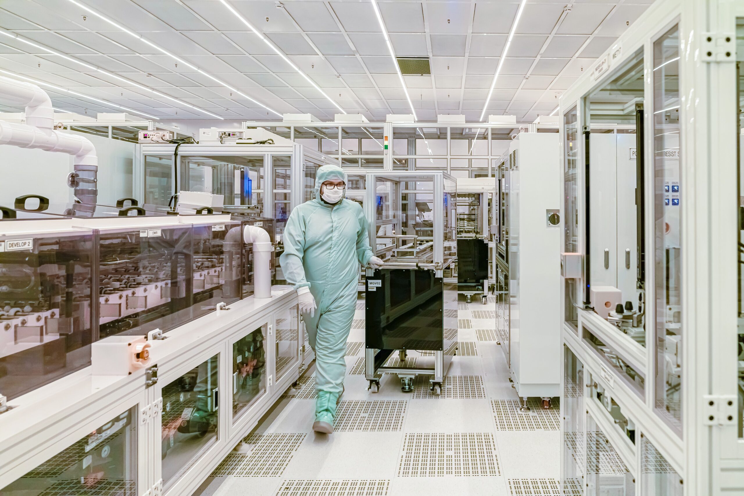
Infineon Technologies has fabricated functional power semiconductor devices on 300mm silicon carbide wafers at its manufacturing facility in Villach, Austria, demonstrating the feasibility of processing the larger substrates using existing silicon fabrication equipment.
The company completed the work in a full-scale semiconductor manufacturing environment, extending silicon carbide processing beyond the 200mm substrate format currently being adopted for commercial production. Infineon has not established a timetable for industrialising the new process or transitioning customers to devices manufactured on 300mm wafers.
Increasing wafer diameter from 200mm to 300mm provides approximately 2.25 times the surface area. Infineon estimates that the larger format can accommodate 2.3 times as many chips per wafer, potentially increasing manufacturing output without a corresponding increase in the number of substrates passing through each compatible fabrication process.
The actual number of usable devices depends on die dimensions, wafer-edge exclusions, process uniformity, and manufacturing yield. A larger substrate increases the area available for semiconductor fabrication, but the economic advantage depends on the proportion of devices meeting electrical specifications after processing.
Silicon carbide is used in power semiconductor applications where high operating voltages, switching losses, and thermal requirements influence the choice of device technology. Compared with conventional silicon, its wide bandgap and higher critical electric field support device structures capable of blocking substantial voltages while maintaining comparatively compact active regions.
These characteristics have contributed to the adoption of SiC MOSFETs in electric vehicle traction inverters, onboard chargers, industrial motor drives, renewable energy converters, and stationary energy storage. Their use can reduce power conversion losses under suitable operating conditions, although the resulting efficiency depends on the complete circuit, switching strategy, and thermal design.
Producing silicon carbide wafers introduces manufacturing constraints that differ from those encountered with silicon. The material is mechanically hard, and growing large crystals with sufficiently low defect densities requires tightly controlled processes. Cutting, grinding, and polishing the substrates can also be expensive and contribute to material loss.
Increasing substrate diameter places additional demands on crystal quality and process consistency. Fabrication equipment must maintain acceptable conditions across a larger surface, while lithography, deposition, etching, and other operations must accommodate the physical and electrical properties of silicon carbide.
Infineon's use of established silicon manufacturing equipment at Villach demonstrates compatibility with elements of the existing fabrication infrastructure. This creates a possible route to expanding SiC production without constructing an entirely separate equipment environment, although the demonstration does not establish that every silicon process can be transferred without modification.
Equipment compatibility must also be distinguished from process qualification. Commercial manufacturing requires repeated production runs demonstrating consistent electrical characteristics, acceptable yields, and device reliability. The initial fabrication of functional power devices establishes a technological milestone rather than confirmation that these requirements have been satisfied.
Infineon is also investigating methods of reducing the amount of silicon carbide lost during substrate preparation. At its Dresden facility in Germany, the company has demonstrated the feasibility of applying its Cold Split technology to 300mm SiC material.
Conventional wafer production commonly involves separating individual slices from a grown crystal, or boule, using wire sawing. The cutting operation removes material, and the resulting surfaces require further preparation before semiconductor devices can be fabricated.
Cold Split is intended to separate wafers with less material loss and reduced processing time. Improving the number of substrates obtained from a single crystal could address part of the cost associated with SiC wafer production, particularly where the starting material is expensive.
The Dresden demonstration establishes that the approach can be applied to the larger format. Infineon has not disclosed commercial yield results, production volumes, or a qualified 300mm substrate supply process based on Cold Split.
Larger wafer area and improved crystal utilisation address different manufacturing costs. Increasing the number of devices processed per wafer may improve equipment productivity, while reducing material loss during wafer separation can improve the use of the grown crystal. Both advantages must be weighed against substrate quality, handling requirements, and the cost of maintaining reliable production.
Wafer-level processing is only one part of semiconductor manufacturing. Devices must subsequently be separated, electrically tested, packaged, and qualified for their intended applications. A process improvement at substrate level does not necessarily produce an equivalent reduction in the cost of a packaged power semiconductor.
Infineon is continuing its established 200mm SiC manufacturing roadmap while assessing the larger format. The company intends to establish future technology and production plans in collaboration with customers and manufacturing partners, rather than committing to an immediate conversion of its existing production lines.
The development follows Infineon's €1.1bn investment in 300mm gallium nitride manufacturing at Villach, announced in October. Although GaN and SiC are both wide bandgap semiconductor materials, their substrates, device architectures, fabrication requirements, and principal applications differ. The latest achievement concerns a separate material platform.
Infineon identifies additional SiC opportunities in AI data centre power systems, including solid-state transformers, electronic circuit protection, and power supplies. Increasing equipment power density and the development of higher-voltage distribution architectures are placing additional demands on semiconductor efficiency and heat removal.
The company will display a processed 300mm SiC wafer at electronica 2026 in Munich from 10 to 13 November. Its next manufacturing milestones will involve repeatable process performance, substrate supply, device qualification, and the establishment of a commercial ramp schedule alongside continued 200mm production.