IN Brief:
- PUFsecurity presented Caliptra and chiplet root-of-trust implementations during the OCP APAC Summit in Taipei.
- Its PUFrt IP combines a NeoPUF-derived device secret, NeoFuse OTP secure storage, and hardware random-number generation.
- The work addresses the physical security primitives required beneath open root-of-trust architectures in AI and chiplet systems.
PUFsecurity has detailed how its hardware security IP can provide device-specific secrets, protected non-volatile storage, and hardware entropy beneath Caliptra root-of-trust implementations for AI servers and chiplet-based systems.
The eMemory subsidiary presented the work during the Open Compute Project APAC Summit in Taipei, including technical discussions around chiplet identity and the implementation of Caliptra in silicon. The focus is on the physical primitives required once an open root-of-trust architecture moves from specification into a manufactured semiconductor.
Caliptra is an Open Compute Project architecture combining hardware IP and firmware for an integrated root of trust. It is intended to establish a trusted layer below higher-level platform firmware, supporting functions including identity, measured boot, attestation, and protection of security material before the main software environment is allowed to take control.
A specification cannot by itself create a unique secret inside a die. The silicon implementation still needs a method of establishing device identity, retaining protected information, and generating unpredictable values for cryptographic operations.
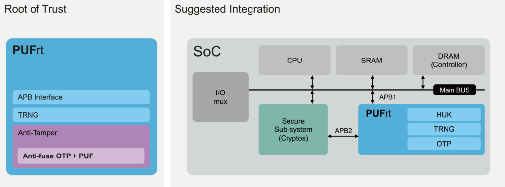
PUFsecurity is positioning its PUFrt IP at that physical layer. The architecture combines NeoPUF, which derives device-specific information from semiconductor manufacturing variation, with NeoFuse one-time-programmable storage and hardware random-number generation.
The company describes its standard PUFrt implementation as including a 1,024-bit physical unclonable function alongside secure storage, entropy generation, and anti-tamper features. The aim is to keep critical identity and key-generation functions within a hardware security boundary rather than relying entirely on secrets programmed externally during manufacturing.
A physical unclonable function uses small process variations that occur naturally between nominally identical integrated circuits. Those variations can be measured to derive a repeatable response associated with a particular die, giving designers a potential device-specific root from which other security credentials can be established.
The technique does not eliminate provisioning or lifecycle management. Semiconductor and system designers still have to determine how device identity is enrolled, which certificates and keys are generated or injected, what information may leave the secure boundary, and how authentication is handled through manufacture, deployment, service, and retirement.
Those questions become more complicated as packages are disaggregated. A monolithic SoC gives the platform architect one principal piece of silicon around which to establish trust. A chiplet-based package can combine compute, accelerators, I/O, memory-related devices, and other dies sourced through different design and manufacturing chains.
Each additional component can create another identity and another interface that may need to be authenticated before the complete package is trusted. The issue is particularly relevant to AI infrastructure, where large systems already combine CPUs, accelerators, networking devices, management controllers, security processors, and firmware from several suppliers.
Caliptra provides a common architectural framework for some of those trust functions, while implementations such as PUFrt attempt to supply the physical semiconductor mechanisms underneath it. The distinction matters because two devices can implement the same higher-level security specification while relying on different methods of storing secrets or establishing device identity.
Hardware roots of trust also carry conventional silicon-design costs. They consume area, interfaces, verification effort, manufacturing test coverage, and power, while the security assumptions have to remain valid as an IP block moves between process technologies and product generations.
For chip designers, the relevant engineering question is therefore not whether an open root-of-trust standard is desirable, but how securely and economically it can be anchored into real silicon. A sophisticated attestation stack still needs an initial secret or identity that an attacker cannot simply copy into another device.
As Caliptra adoption broadens, that underlying implementation will attract more scrutiny. Open firmware can define what should be measured and verified; the semiconductor industry still has to provide a trustworthy physical point from which that chain begins.