IN Brief:
- AI clusters are increasing pressure on electrical links as bandwidth, power density, and system scale rise.
- Co-packaged optics moves optical conversion closer to switch and compute silicon, changing packaging, thermal, manufacturing, and test requirements.
- UK capability spans InP materials, silicon photonics prototyping, advanced packaging, and test, although commercial scale remains the harder challenge.
The rapid expansion of artificial intelligence infrastructure is being felt well beyond processor design. IQE, headquartered in Cardiff, expects first half 2026 revenue of at least £64 million after demand accelerated across its core markets, with indium phosphide products for data centre and AI photonics emerging as a major growth driver. The company has lifted its revenue growth guidance for the full year to more than 30 per cent.
The figures put an industrial measure on a change that is increasingly visible across advanced computing. AI accelerators can only deliver useful performance if enormous volumes of data can move between processors, memory, and network switches quickly enough to keep the silicon occupied. As clusters grow and lane rates rise, the electrical links carrying that traffic face higher losses, greater power requirements, tighter routing constraints, and increasing thermal pressure.
Copper is not disappearing, but maintaining signal integrity over demanding links requires equalisation, retiming, clocking, and careful channel design, consuming power and package or board space. Optical fibre changes the relationship between bandwidth and reach, carrying large quantities of data without the same electrical channel loss.
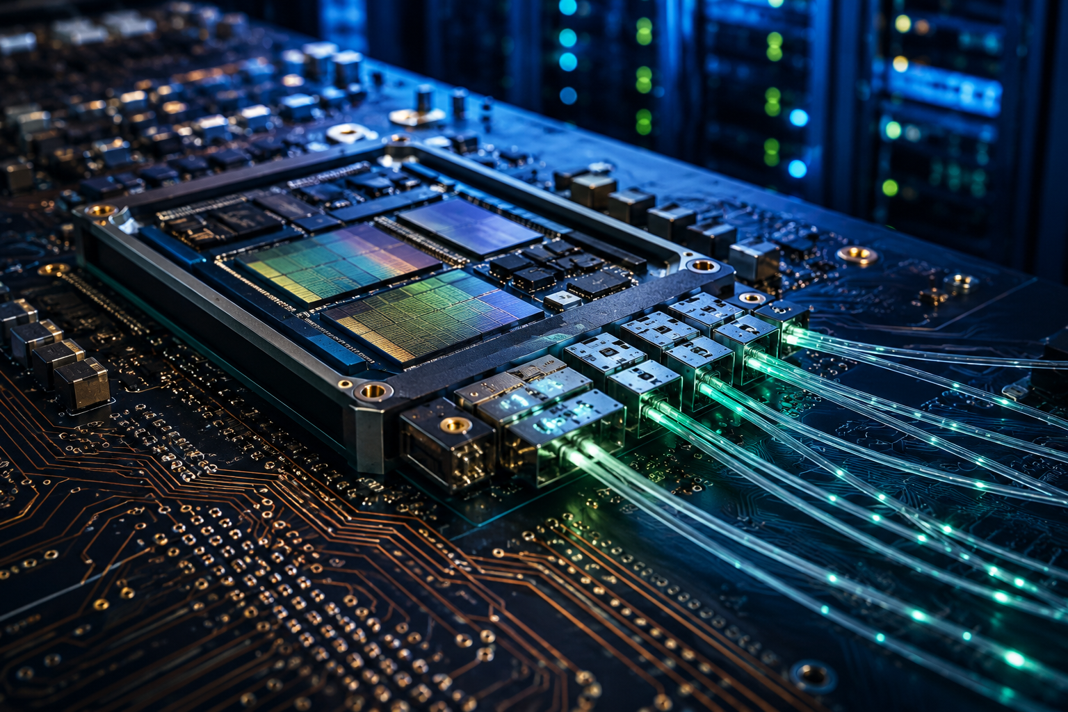
Historically, much of the conversion from electrical to optical signals in data centres has taken place in pluggable transceiver modules at the edge of a switch or server. Moving the optical engine towards the package, and ultimately adopting co-packaged optics, shortens the most demanding electrical path by placing conversion much closer to the switching or compute silicon. That approach is now entering commercial system roadmaps rather than remaining confined to research demonstrations.
Moving the optical boundary
NVIDIA’s Spectrum-X Ethernet Photonics architecture is one prominent example. Its co-packaged optical designs integrate silicon photonics with the switching ASIC and scale to as much as 409.6Tb/s of total switch bandwidth in the SN6800-LD configuration. NVIDIA has also moved Spectrum-X Ethernet Photonics into the Vera Rubin production programme, with the photonics switches scheduled for availability during the second half of 2026.
The pressure extends beyond rack networking. ZeroPoint Technologies’ ZeroStream puts lossless compression into processor and accelerator memory paths, targeting another bandwidth constraint in AI accelerators, CPUs, and networking SoCs. Compression and optical interconnect address different parts of the architecture, but both reduce the growing cost of moving data.
Bringing optical conversion closer to the processor does not simply exchange a copper connection for fibre. It changes the materials, packaging, thermal, manufacturing, and test decisions surrounding the device. Silicon photonics provides a route to fabricate waveguides, modulators, detectors, and other optical structures using processes compatible with semiconductor manufacturing, but silicon is not an efficient light emitter.
That leaves an important role for compound semiconductors, particularly indium phosphide, in lasers and other active optical functions. IQE and Tower Semiconductor signed an agreement spanning multiple years in June under which IQE will provide InP epiwafers for Tower’s silicon photonics platforms. The work covers technology for 200Gb/s per lane pluggable transceivers, prototype 400Gb/s per lane modulators, and optical circuit switches for data centre deployment.
The combination illustrates why heterogeneous integration is becoming increasingly important. Silicon offers mature manufacturing and dense electronic integration, while III-V materials provide optical and high frequency properties that silicon cannot easily match. Combining them at package or interposer level allows each material system to be used where it performs best.
The same integration logic is appearing in adjacent semiconductor development. Imec has extended its 300mm RF silicon interposer for III-V chiplet integration with Si-CMOS, adding embedded capacitors, passive modelling, and laser assisted bonding. The platform is aimed at mmWave, sub-THz, and ultrafast data centre applications, and its assembly work has demonstrated alignment accuracy below 600nm across a 43-device test set.
Once several material systems and interfaces share one assembly, packaging becomes part of the electrical and optical architecture. Optical dies and fibres require tight alignment, while electronic and photonic components can have different thermal limits and ageing behaviour. A switch ASIC with a high power density may sit only millimetres from temperature sensitive optical elements, bringing cooling and mechanical stability into the same design exercise.
Manufacturing yield also becomes harder to manage when electronic dies, photonic dies, optical interfaces, and packaging steps are combined. Screening before assembly, fibre attachment, connector design, and optical test all influence the economics of the finished system. Fault isolation and field service also become more complicated when optics is integrated beside switching silicon.
Those constraints are one reason co-packaged optics will not automatically displace pluggable transceivers across every application. Pluggables are mature, replaceable, and operationally familiar, while tighter integration can reduce electrical reach and raise bandwidth density at the cost of more demanding package design and serviceability. The architectural balance will depend on bandwidth, power, reach, reliability, and maintenance requirements rather than a single performance metric.
Materials, packaging and the UK opportunity
The UK already holds useful positions across several parts of the emerging stack. IQE’s InP manufacturing capability is one, and in July the company secured a $14 million production order for AI and data centre applications from a global technology customer. Production will take place at Newport, adding volume manufacturing activity to a photonics market often discussed primarily through research capability and design expertise.
At the University of Southampton, CORNERSTONE operates a silicon photonics rapid prototyping foundry with open access to platforms including silicon on insulator, silicon nitride, suspended silicon, and germanium on silicon. Multi-project wafer runs and industry compatible deep ultraviolet projection lithography provide a route from early prototyping towards processes designed with subsequent scale in mind.
The support structure around commercialisation is also broadening. The transition of the Compound Semiconductor Applications Catapult into the Semiconductor Catapult expands its remit across semiconductor R&D, validation, commercialisation, and AI hardware deployment. Existing capabilities include photonics characterisation, advanced packaging, thermal management, assembly, integration, and test.
Those assets do not amount to a complete domestic optical interconnect supply chain. Commercial deployment still depends on dependable wafer supply, device fabrication, laser sources, packaging processes, fibres, connectors, test equipment, and assembly capacity, all operating at yields and costs that work for data centre volumes. Scaling a photonic technology from a successful demonstrator into thousands of reliable optical engines is a manufacturing problem as much as an optical one.
The resulting opportunity is therefore wider than ownership of a leading AI processor architecture. Materials, photonic integrated circuits, packaging, test, specialist manufacturing, and system integration all sit between the compute die and the fibre carrying its data, and each has to operate within increasingly tight power and thermal budgets.
As lane speeds rise and AI clusters become larger, the point at which electrical signalling hands data to optics is moving closer to the silicon doing the computation. Exactly how close will vary with architecture, cost, and service model. Once the optical engine reaches the package, however, fibre coupling, thermal behaviour, materials, reliability, and optical test become part of the electronics design brief itself.