IN Brief:
- Silicon Box has advanced a €3.2bn Novara plant for panel-level semiconductor packaging and test, backed in part by approved public funding.
- Basic design covers cleanroom systems, equipment flows, building services, water use, and process heat recovery.
- Construction is planned for 2027; the Commission has identified 2033 as a full-capacity target, not a confirmed production start.
Silicon Box has moved its proposed €3.2 billion advanced semiconductor assembly and test facility in Novara, northern Italy, into the basic design phase, bringing the engineering of the plant’s production areas and supporting infrastructure into focus. Stantec and Drees & Sommer are working with the Singapore-based semiconductor packaging company on the project, which is intended to establish a new European capability for integrating multiple chiplets into finished packages.
The Vulcan Project was presented in Novara on 9 November, after Italian authorities confirmed a €3.2 billion investment programme that includes €1.3 billion in approved public support. The proposal anticipates about 1,600 direct skilled jobs once the site develops. Construction is planned for the opening months of 2027, although a firm commissioning or commercial production date has not been disclosed.
The planned factory will undertake the back-end stages of semiconductor manufacturing — assembly, advanced packaging, and testing — rather than the front-end fabrication of transistors on silicon wafers. It would integrate completed dies from potentially different manufacturers into multi-chip packages, allowing separate functions to be combined without manufacturing them all on one large silicon die.
Silicon Box’s approach uses advanced panel-level packaging, in which multiple units can be processed across a larger panel rather than exclusively on individual circular wafers. Precise die placement, alignment, redistribution-layer formation, interconnection integrity, and final inspection are among the engineering tasks that influence yield and package reliability. The company has not published a Novara production capacity, detailed tool list, or guaranteed yield for the planned Italian installation.
Processing large panels places demanding requirements on factory layout and utilities. Production equipment must move substrates through controlled process areas while maintaining appropriate cleanliness, temperature, humidity, and contamination controls. Power quality, ventilation, chemical handling, and process water affect the repeatability of individual tools; allowing room for later equipment changes is another part of the design challenge.
Stantec is responsible for project coordination, infrastructure, permits, the office building, and external areas, while Drees & Sommer is designing the production and utility buildings, including cleanroom systems. Their respective disciplines have to meet at the boundaries between tools, buildings, and utilities: inefficient material routes, limited maintenance access, or poorly positioned service connections can be difficult to remedy after installation.
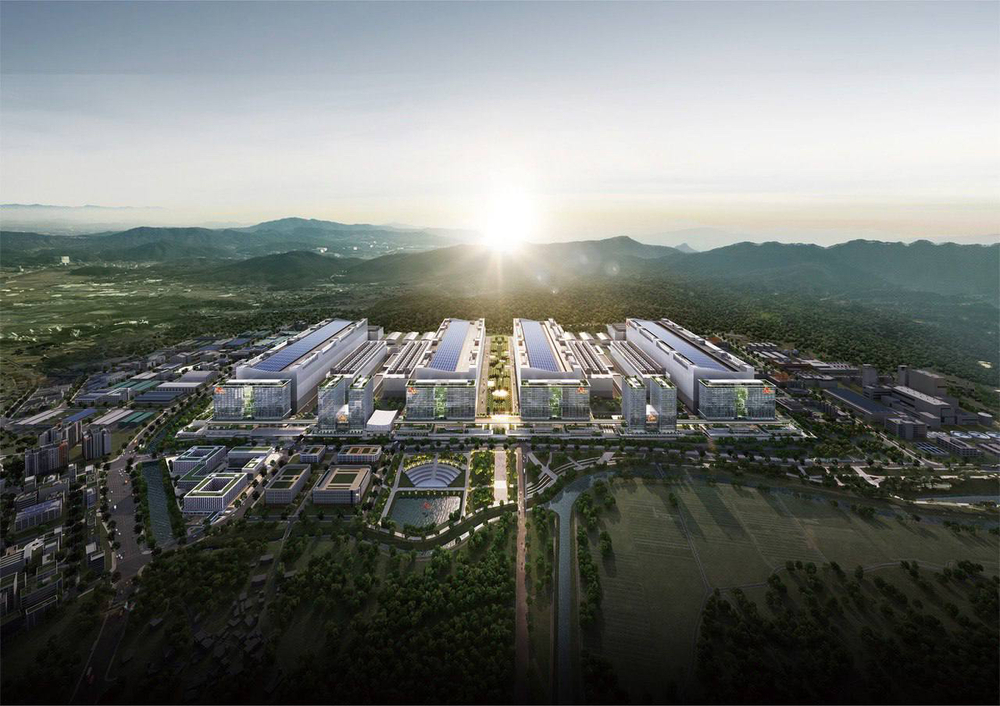
The proposed campus occupies about 60 hectares in the province of Novara, near the Agognate railway station. Its wider plan incorporates stormwater management, soil permeability, and landscape measures alongside the industrial buildings. These site features do not remove the substantial energy, cooling, and water demands of semiconductor processing, making the detailed utility design particularly consequential before the plant can be equipped.
Stantec proposes water reuse, process heat recovery, and photovoltaic generation, alongside landscape and stormwater measures across the site. These remain design intentions rather than measured reductions in energy or water use. Recoverable heat depends on equipment operating temperatures and usable local loads, while water recycling depends on the cleanliness required by each process and the treatment systems ultimately installed.
Package assembly also requires close coordination with customers’ chip designs and upstream fabrication choices. Die thickness, interconnect pitch, thermal characteristics, substrate compatibility, and test access need to be resolved as part of a package architecture. A plant serving several device categories will require process controls and quality systems capable of handling those differing requirements without conflating one qualified process with another.
Silicon Box has already developed high-volume panel-level packaging at its Singapore operation. The company has said that more than one billion units have been shipped there, providing a commercial production reference for the broader technology. That track record does not establish how quickly the proposed Novara plant could reproduce equivalent throughput, particularly while its layout, utilities, equipment, and workforce arrangements remain under development.
The European Commission granted the proposed Novara facility Open EU Foundry status under the Chips Act in March 2026. The designation recognises a first-of-a-kind semiconductor capability and provides a framework for administrative support and access to relevant European initiatives; it does not mean that the factory is operational. The Commission has previously referred to a full-capacity target of 2033, distinct from the planned start of construction in 2027.
Before any assembly line can begin qualified output, the basic design will need to be translated into construction work, equipment specifications, installation, and process validation. Silicon Box has confirmed the design transition and a 2027 construction intention, but has not given a tool-by-tool delivery schedule or committed date for the first commercially qualified packages from Novara.