IN Brief:
- MasterGaN7 combines two 650V enhancement-mode GaN transistors with high-voltage gate driving and protection.
- The device has a 6A maximum transistor current rating, 270mΩ typical on-resistance and switching capability up to 2MHz.
- ST has started volume production in a 9mm QFN package, with the EVLMG7 evaluation board available.
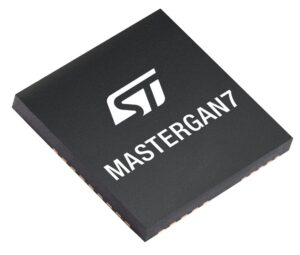
STMicroelectronics has extended its MasterGaN power family with MasterGaN7, a device containing two 650V enhancement-mode gallium nitride transistors and a high-voltage gate driver in a single package. The company has started volume production of the integrated half-bridge, which supports transistor current ratings up to 6A and switching frequencies up to 2MHz. Applications include chargers, power adapters, industrial lighting and solar microinverters.
Both GaN transistors have a typical on-state resistance of 270 milliohms and share a compact 9mm by 9mm QFN package with the drive and protection electronics. Integration removes some of the separate driver circuitry otherwise needed around a discrete power stage. ST also provides compatible pin assignments and footprint dimensions within its wider MasterGaN family, although a replacement design must still be checked against the electrical and thermal characteristics of the selected device.
The transistors form a half-bridge, allowing a controller to switch the midpoint between high and low supply rails. Such an arrangement appears in several power conversion topologies, including resonant converters and inverter stages. The 650V figure describes the drain-source blocking capability of the switches; it does not define a universal continuous bus voltage or converter output rating. Those limits depend on the circuit arrangement, transient overshoot, operating conditions and required design margins.
Gate drive timing is particularly important when fast semiconductor devices share a half-bridge. If the upper and lower switches conduct simultaneously, a large current can flow between the supply rails. MasterGaN7 includes an interlocking function intended to prevent this cross-conduction condition, alongside undervoltage lockout and thermal shutdown protection. The surrounding power stage still requires appropriate current protection, cooling and system-level fault handling.
ST specifies an overall driver propagation delay of 45 nanoseconds and a minimum pulse duration of 35 nanoseconds. These short intervals allow the half-bridge to operate at high switching frequencies, although the maximum stated 2MHz capability is not an efficiency result for every converter topology. Actual switching frequency must be chosen against magnetic component losses, semiconductor heating, electromagnetic interference and the available control resolution.
Increasing switching frequency can reduce the energy that inductors and capacitors must store during each cycle, potentially allowing smaller magnetic and passive components. That advantage comes with additional switching events and greater sensitivity to parasitic inductance and capacitance. Circuit layout, current loops and thermal paths remain consequential even when the driver and transistors are placed inside the same package.
The new device adds low dropout regulators on both driver supply sections. These regulate the voltage available to the gate driving circuits, helping maintain suitable operating conditions as the power stage switches. An integrated bootstrap diode supplies the floating high-side driver, while externally adjustable turn-on resistors allow the designer to influence switching transitions and balance speed against unwanted electrical emissions.
Separate standby and shutdown controls support operation at light loads and during inactive periods. The integrated standby function reduces the device’s power consumption when switching is not needed, and a fast wake-up mechanism supports its return to normal operation. A fault output provides a means of conveying device status to the controller. The system must still distinguish a reported fault from other possible causes of converter malfunction.
MasterGaN7 is specified for operation across an industrial temperature range from -40°C to +125°C. The compact package can simplify component placement, but its thermal performance depends on the printed circuit board, copper areas, switching losses and cooling arrangement. The 6A maximum current rating and typical resistance should therefore be assessed alongside the converter’s actual operating waveform and heat dissipation rather than used alone to infer continuous delivered power.
ST lists several converter arrangements across the MasterGaN family, including active clamp flyback, asymmetrical half-bridge and resonant LLC designs, as well as DC-to-AC inverters. MasterGaN7 offers integrated switching hardware for such designs, with supporting passive components and controls remaining external. Its pin compatibility with other family members creates a possible reuse route for existing layouts, subject to a full component-level design check.
The device is available in volume production, with indicative pricing starting at $3.83 for orders of 1,000 units. ST also offers the EVLMG7 evaluation board to support development work. These availability details distinguish the launch from a research demonstrator, while final efficiency, power density and electromagnetic performance remain characteristics of the converter built around the device.