
IN Brief:
- Thintronics has won Junkosha’s microwave and millimetre-wave technology innovator category.
- The company’s isotropic, skew-free, low-loss, low-Dk dielectric materials target boards, packages, and semiconductor interconnects.
- AI infrastructure is placing new pressure on materials used in high-frequency data channels and advanced interconnect stacks.
Thintronics has been named winner of Junkosha’s microwave and millimetre-wave Technology Innovator of the Year category for its low-loss dielectric materials.
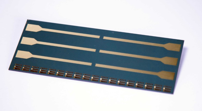
The California-based electronic materials company has developed isotropic, skew-free, low-loss, low-Dk dielectric materials intended for use as insulation layers across boards, packages, and semiconductor interconnect structures.
The materials are designed to reduce dielectric loss, suppress signal degradation, and improve power efficiency in high-frequency data channels. Conventional polymers and laminates are reaching performance ceilings in AI infrastructure, high-performance computing, networking, and large-scale data centre systems.
Dielectric materials are often hidden inside the electronics stack, yet their influence grows sharply at higher frequencies and longer channel lengths. Loss tangent, dielectric constant, skew, moisture absorption, thermal behaviour, manufacturability, and compatibility with copper structures all affect how far and how efficiently signals can travel.
Interconnect performance is now one of the constraints on AI system scaling. Processors, accelerators, memory devices, optical interfaces, and power delivery networks attract most of the attention, but high-speed electrical channels still depend on materials that can preserve signal integrity while supporting dense routing.
The award points to a larger materials challenge inside advanced electronics. As data rates rise, losses in the board and package substrate become part of the energy budget. Lower signal loss can reduce the burden on equalisation, retiming, drive strength, cooling, and system power.
Materials supply is already under pressure from AI infrastructure growth, with SEMI warning of increased strain across critical electronics inputs. Thintronics’ work sits directly within that environment. AI demand is increasing requirements not only for leading-edge logic and memory, but also for the materials that connect devices together.
The same pattern is visible in semiconductor scaling and packaging. Sub-one-nanometre logic research highlights density and energy efficiency at transistor level, but package and board interconnects must advance in parallel if those gains are to be useful in system-level hardware.
Materials engineering is also becoming more closely linked to supply-chain strategy. New dielectrics must be manufacturable at scale, compatible with existing fabrication flows where possible, and available in forms that board makers, substrate manufacturers, and packaging suppliers can qualify. A material breakthrough becomes commercially relevant only when it fits design rules, process windows, reliability testing, and procurement models.
High-speed channel planning increasingly requires early collaboration between silicon teams, package engineers, PCB designers, materials suppliers, and system architects. The separation between component selection and board material selection is weakening as losses, heat, and data movement become shared constraints.
Thintronics’ recognition signals the rising importance of dielectric innovation in AI-era electronics. Customer qualification, volume readiness, and integration across package and board structures will determine how far low-Dk materials can move into the next generation of compute and networking platforms.

