IN Brief:
- AOI has placed a multi-year, multi-million-dollar order with Trymax for semiconductor processing equipment.
- The systems support plasma ashing and UV curing within AOI’s in-house InP laser manufacturing operation.
- The investment adds upstream wafer-processing capacity as AOI expands 800G and 1.6T optical transceiver production.
Trymax Semiconductor Equipment has secured a multi-year, multi-million-dollar order from Applied Optoelectronics Inc (AOI) for plasma ashing and ultraviolet curing equipment used in indium phosphide laser production. The systems will be deployed at AOI’s wafer fabrication operation in Sugar Land, Texas, where the company manufactures InP laser chips for high-speed optical transceivers.
The order covers equipment for process steps carried out before the lasers reach transceiver assembly. Plasma ashing removes photoresist and process residues after lithography or etching, while UV curing can stabilise resist and erase accumulated charge. Trymax has not disclosed the exact tool configuration ordered by AOI, so the contract represents a process-capacity investment rather than a model-specific equipment launch.
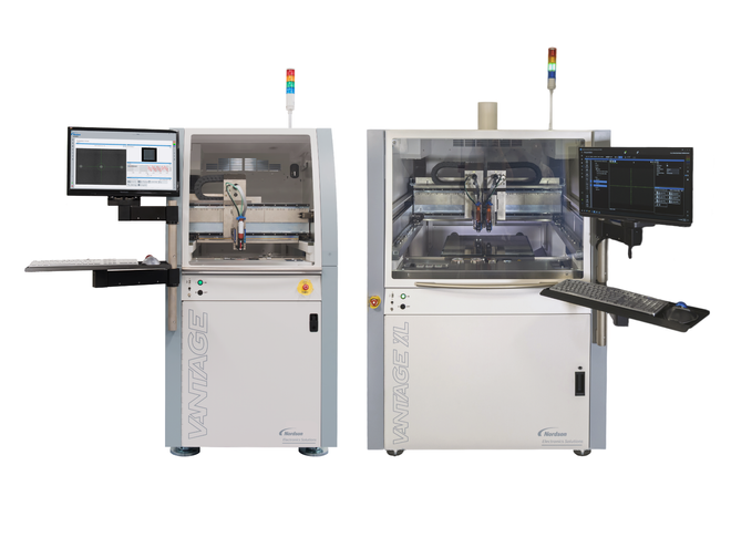
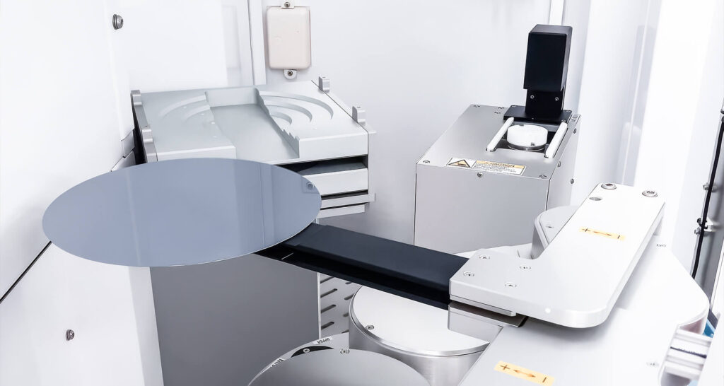
Trymax’s NEO platform supports semiconductor substrates across several materials and wafer sizes, including compound semiconductors. Its NEO 2000 family handles 100 mm, 150 mm, and 200 mm substrates for plasma ashing, descum, light etching, surface preparation, and cleaning. The NEO 2000UV is a dual-chamber UV curing and charge-erase system designed for substrates up to 200 mm.
Indium phosphide is used for emitters and photonic devices operating at wavelengths suited to fibre-optic communications. Compared with mainstream silicon processing, compound semiconductor wafers can impose different mechanical and process constraints, including greater fragility and more specialised handling. Residue removal and surface treatment also have to be controlled closely because later deposition, coating, bonding, and lithographic steps depend on a clean and repeatable surface condition.
Plasma ashing is mature technology, but the useful operating window can narrow as structures become smaller or materials more sensitive. The process has to remove resist and polymer residues without attacking the underlying device, altering critical dimensions, or leaving contamination that affects later layers. Trymax offers microwave downstream, RF bias, and dual-source plasma configurations across its broader NEO range, allowing process conditions to be adapted to the substrate and application.
UV curing serves a different part of the flow. Controlled irradiation can photo-stabilise resist before implantation or etching and can neutralise charge that has built up during device processing. Trymax’s NEO 2000UV uses variable irradiance control and automated wafer handling, with the platform also supporting fab-host communications through SECS-II.
The AOI order arrives during a large expansion in optical transceiver output. AOI has said its manufacturing capacity is approaching 200,000 units per month and expects capacity for 800G and 1.6T products to reach around 650,000 units per month by the end of 2026. The company is also adding manufacturing space in Texas as AI and cloud customers increase demand for high-speed optical links.
That expansion reaches further upstream than final module assembly. An 800G or 1.6T transceiver depends on lasers, drivers, receivers, photonic components, fibre interfaces, alignment, packaging, and test, so higher shipment volumes eventually require more wafer-level capability as well. AOI’s in-house laser production means the capacity of its InP process line directly influences how quickly finished transceiver output can increase.
Yield becomes especially important as that line scales. A production problem early in wafer fabrication can remove multiple potential devices before packaging and test, while unstable process conditions can create variation that only becomes visible later in optical performance. Additional ashing and curing equipment therefore contributes to throughput while helping AOI maintain repeatable surface preparation and resist behaviour as volumes rise.
The highest-profile spending around AI networks remains concentrated on accelerators, switches, and optical modules, but those products depend on specialist manufacturing processes scaling at the same rate. AOI’s capacity programme now extends into the less conspicuous wafer-processing stages that determine whether enough qualified InP laser devices are available for the later transceiver lines.