IN Brief:
- WiseWare digital control will be paired with Navitas GaN and SiC technologies for high power computing applications.
- Initial work targets AI data centre power supplies and other grid-to-chip conversion topologies.
- The collaboration will test how real-time control and wide bandgap switching can improve efficiency, density, and transient performance.
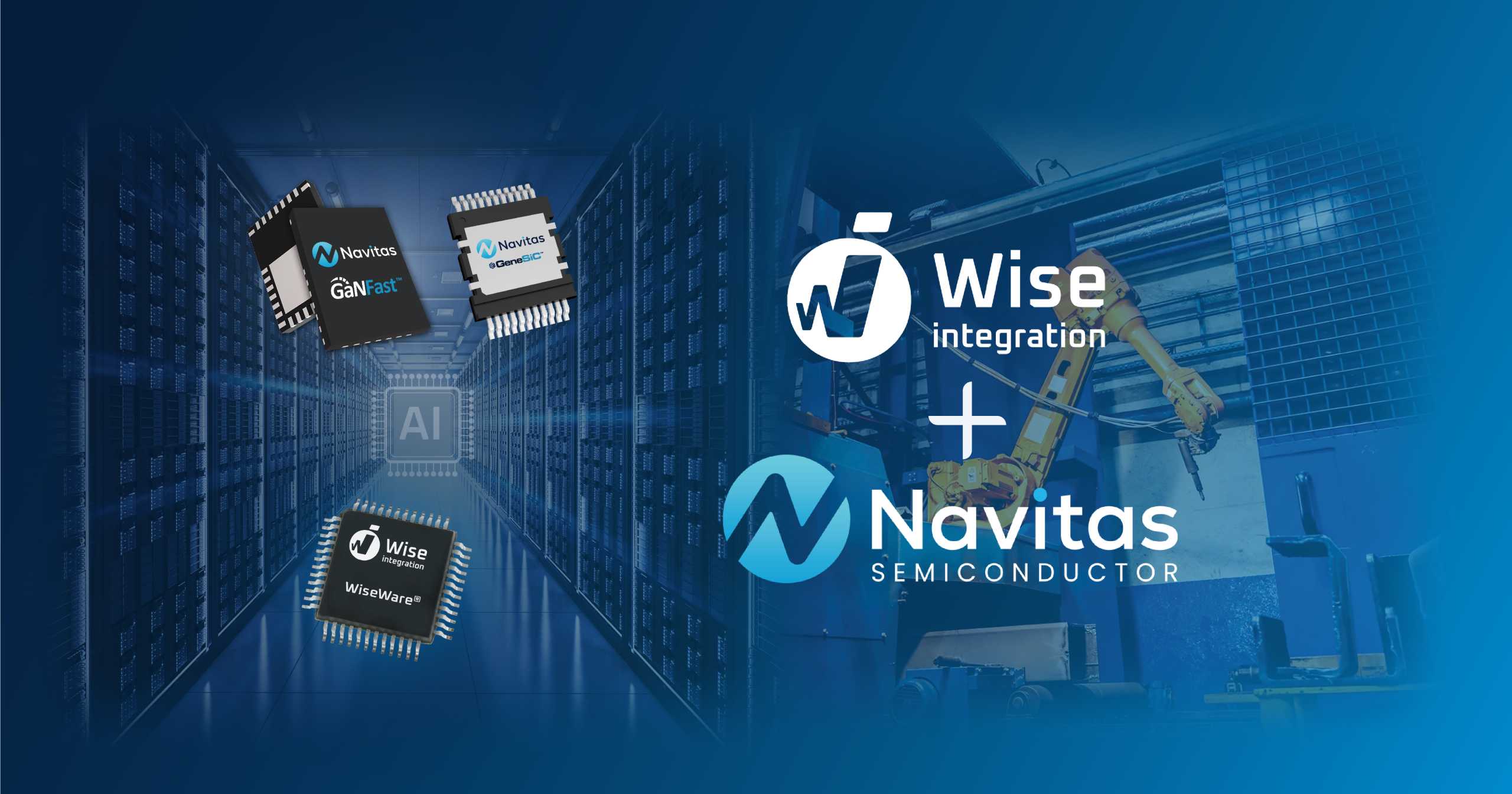
Wise Integration and Navitas Semiconductor have agreed to combine distributed digital power control with gallium nitride and silicon carbide devices for high performance computing power systems, beginning with AI data centre power supplies and extending to wider grid-to-chip conversion architectures.
The collaboration brings Wise Integration’s WiseWare control technology together with Navitas’s GaN and SiC semiconductor portfolio. The companies plan to examine power conversion topologies across the path from incoming supply to processor, where rising rack power and tighter efficiency targets are increasing the electrical and thermal burden on each conversion stage.
WiseWare provides real-time digital control of power conversion rather than relying solely on conventional analogue control loops. In wide bandgap converters, that control layer has to manage switching behaviour, transient response, protection, and system stability while the faster devices place tighter constraints on timing, magnetics, layout, and thermal design.
Navitas contributes GaN and SiC technologies for different parts of that conversion chain. GaN is attractive where higher switching frequency and compact passive components are priorities, while SiC is established in higher voltage stages where conduction loss, switching loss, and thermal performance have to be balanced at greater power levels. Using both device families allows each conversion stage to be matched to its electrical requirements rather than forcing one technology across the entire architecture.
The first target is AI data centre power infrastructure, with AI PCs, high-end workstations, gaming desktops, and industrial systems also identified as applications. Accelerator based computing has pushed rack power sharply upwards, increasing losses and cooling demand while shrinking the physical space available for power electronics. That pressure is driving work on 800VDC distribution, solid-state transformers, higher frequency conversion, and more direct conversion between grid input and processor rails.
As those architectures become more complex, coordination between stages becomes more important. A digital controller can alter switching behaviour using operating data and software-defined control logic, allowing the converter to respond to changing loads and operating conditions. The engineering challenge is to gain that flexibility without introducing latency, instability, or unnecessary processing overhead during fast load steps.
Navitas has also been expanding its silicon carbide position through a separate $5 million investment in Magnachip, linked to the transfer and qualification of higher voltage GeneSiC technology in South Korea. The Wise Integration agreement addresses a different part of the value chain, connecting power devices with the control layer needed to turn switching performance into a complete converter design.
Wide bandgap devices alone do not guarantee a denser or more efficient system. Gate drive, dead time, switching frequency, magnetic design, parasitic inductance, thermal paths, protection, and firmware all influence the result. Combining device development with digital control gives the partners a route to optimise those variables together instead of treating the semiconductor and control stages as separate design problems.
No production programme, reference platform, or availability date has yet been announced. Hardware demonstrations will need to show which topologies are being pursued, where GaN and SiC are used, and how the resulting systems perform on efficiency, power density, transient response, and thermal behaviour.
The collaboration also sits against a shift in server power design from centralised conversion towards architectures that push higher voltage closer to the load. Fewer conversion stages can reduce cumulative loss, but each remaining stage has to handle a wider operating envelope and more aggressive transients. That increases the value of control schemes able to coordinate switching behaviour across changing load, input, and thermal conditions without sacrificing protection margins.
Those measurements will determine how far the collaboration progresses beyond a technology agreement. AI infrastructure is creating a demanding test environment for new power architectures, and any practical advantage will have to survive the full converter design, including magnetics, cooling, protection, and control, rather than appearing only in device-level efficiency figures.