
IN Brief:
- ASML recorded second-quarter net sales of €9.3bn and net income of €2.9bn.
- Full-year sales are now expected to reach €43bn to €45bn, with a gross margin of 54% to 56%.
- Advanced logic, high-bandwidth memory, and AI infrastructure are drawing further investment into leading-edge manufacturing capacity.
ASML has raised its full-year sales outlook after reporting second-quarter net sales of €9.3bn and net income of €2.9bn, as semiconductor manufacturers accelerate investment in advanced logic and memory capacity for artificial intelligence infrastructure.
The Dutch lithography equipment manufacturer now expects 2026 net sales of between €43bn and €45bn, with a gross margin of 54% to 56%. Order activity is being supported by demand for the systems used to manufacture leading-edge processors, high-bandwidth memory, and the supporting silicon required across data-centre platforms.
AI accelerators have increased the amount of silicon deployed within each computing system, while also placing greater demands on memory bandwidth, high-speed interconnects, power management, and advanced packaging. Investment is consequently extending beyond processor wafers into several connected manufacturing chains, each of which depends on additional lithography, deposition, etch, metrology, and inspection capacity.
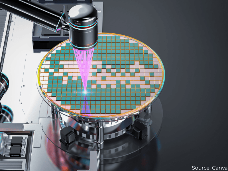
Extreme ultraviolet lithography remains central to advanced-node production because it enables smaller features to be patterned with fewer process steps than would otherwise be required through multiple-patterning techniques. Deep ultraviolet equipment continues to carry a substantial share of demand, particularly across mature layers, supporting devices, and the less geometrically demanding stages of advanced processes.
High-bandwidth memory is becoming an increasingly significant source of equipment demand. HBM devices place several DRAM dies close to an accelerator, using through-silicon vias and advanced bonding to deliver the data rates needed to keep large processing arrays occupied. Greater output therefore requires additional front-end wafer capacity alongside wafer thinning, bonding, assembly, and test equipment.
Although processor production receives much of the attention surrounding AI investment, shortages in memory or packaging can restrict the number of complete accelerator modules shipped. A surplus of logic wafers offers little benefit when suitable memory stacks, substrates, optical interfaces, or thermal components remain unavailable.
Expanding lithography output presents its own constraints. Each system depends on specialist optics, light sources, precision motion assemblies, vacuum equipment, control electronics, metrology, and software, with several critical parts supplied by companies whose production cannot be increased quickly. Additional final-assembly capacity must therefore be matched throughout the supplier base.
Much of ASML’s available EUV capacity for 2027 is already committed, while preparations are under way to increase annual system output over the following two years. Equipment lead times mean that purchases made during the current investment cycle will shape semiconductor capacity well beyond the immediate period of AI infrastructure spending.
A lithography tool also remains productive only when supported by field service, replacement modules, calibration equipment, and qualified technicians. As the installed base expands across several continents, maintaining uptime will require parallel growth in service infrastructure and a larger pool of engineers capable of working on equipment built to nanometre-scale tolerances.
Metrology has become equally critical as features shrink and devices adopt more complex three-dimensional structures. Overlay, critical dimensions, and defect levels must be controlled across a growing number of process steps, prompting further investment in high-resolution inspection. Dutch semiconductor activity has extended into this area through additional funding for advanced process-control technology.
Across Europe, research programmes are preparing manufacturing methods for the generations that will follow current leading-edge devices. A TNO and ASML photonic-chip pilot line is intended to move integrated photonics towards repeatable production, while Imec’s 300mm integration work on two-dimensional transistor materials is addressing device structures that could extend scaling beyond conventional silicon channels.
Those programmes also illustrate how semiconductor progress now depends on several technologies advancing together. Higher transistor density must be accompanied by improvements in memory, optical connectivity, packaging, cooling, and power delivery, otherwise performance gains at device level are lost elsewhere in the system.
Capital commitments of this scale carry substantial exposure. A leading-edge fabrication plant can take several years to build, equip, qualify, and ramp, by which point demand assumptions may have changed. Manufacturers must balance the risk of insufficient capacity against the financial consequences of facilities operating below their intended utilisation.
With equipment bookings extending into later years, ASML’s raised forecast points to a prolonged manufacturing build-out rather than a brief increase in tool orders. The pace of expansion will depend on whether lithography suppliers, memory producers, packaging houses, and materials companies can increase output without introducing fresh constraints elsewhere in the production chain.

