IN Brief:
- The collaboration addresses design and manufacturing challenges for vertically stacked nanosheet transistor research.
- IBM plans an early research process design kit for its nanostack architecture in the first quarter of 2027.
- No commercial manufacturing process or production-ready transistor has been announced.
IBM and Siemens have announced research into the design and manufacturing requirements of IBM’s nanostack transistor architecture. The work brings together semiconductor device research, electronic design automation, process simulation and lithography modelling to investigate whether vertically stacked nanosheet structures can eventually be manufactured at scale. Neither company has announced a production-qualified nanostack process or a timetable for commercial chip shipments.
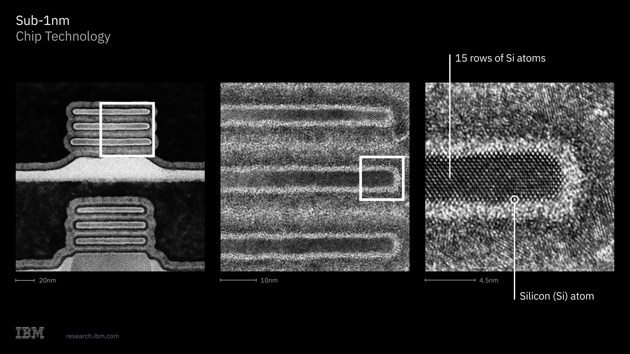
Nanostack extends the nanosheet transistor concept by arranging and staggering transistor structures at different vertical levels. Conventional scaling has largely sought higher device density by reducing lateral dimensions and improving circuit layout. Moving functional transistor structures into a third dimension creates another possible route to density improvements, but introduces fabrication and interconnection challenges that cannot be resolved by a device demonstration alone.
IBM has reported early research results for its seven-angstrom technology-node architecture and describes potential benefits for logic density, power efficiency and static random-access memory. These are research claims associated with a proposed architecture, not independent evidence of a stable, high-volume manufacturing process. The node designation also should not be read as a direct measurement of a transistor’s physical gate length or another single feature.
The collaboration will develop virtual models for assessing device operation and proposed manufacturing sequences. A change intended to improve electrical behaviour can influence patterning difficulty, material interfaces, parasitic resistance or capacitance. Those effects must be considered together because a geometry that performs well in an isolated simulation may be difficult to replicate reliably across a wafer containing many billions of interconnected devices.
Stacking devices creates additional questions about access to individual layers during fabrication. Lithographic alignment, deposition uniformity, isolation, thermal processing and contact formation must be managed without damaging structures already completed below. Designers also need electrical models that describe coupling between neighbouring conductors and the effects of heat generated within a denser arrangement. These are precisely the types of interactions that process and circuit simulation are intended to expose before repeated fabrication experiments.
Siemens is contributing expertise in EDA software, lithography optimisation and advanced manufacturing simulation. IBM’s device researchers provide the proposed structures and associated experimental findings. The joint work is intended to connect what the device design requires with what a feasible process sequence might deliver. A virtual result can guide experiments, but final validation still requires fabricated devices, reliability testing and demonstrated process yield.
A separate IBM research announcement dated 13 October outlined plans to make an early nanostack process design kit available during the first quarter of 2027. Such a kit provides design rules and models that allow circuit developers to assess how an architecture could support actual designs. Its planned research status is important: it is not a released foundry PDK or evidence that designers can submit production-ready nanostack chips for manufacture today.
Early access to models could allow device, circuit and tooling specialists to identify incompatibilities before a process reaches an advanced development stage. Accurate timing, power and layout checks depend on models that track the measured behaviour of the underlying devices. As experiments improve, the kit’s contents would need to change to reflect new restrictions, parasitic effects and fabrication limits.
Vertically integrated semiconductor structures may allow different channel materials or device characteristics to be explored at separate levels. That flexibility adds variables to manufacturing and design optimisation, especially if each layer requires different thermal or processing conditions. Establishing a manufacturable technology therefore depends on consistent material quality, interconnect access, circuit verification and repeatability across complete wafers.
IBM and Siemens have positioned their agreement as research aimed at closing these gaps. Further public evidence will be needed on device reliability, patterning, process yield and integrated-circuit results before the technology can be described as a commercially manufacturable transistor platform.