IN Brief:
- Infineon's 40V OptiMOS 7 devices target high-frequency DC-DC conversion in computing and telecommunications equipment.
- Switching-optimised devices offer improved electrical figures of merit alongside source-down and dual-side cooling options.
- The portfolio is in mass production, with package options measuring 3.3 × 3.3mm and 5 × 6mm.
Infineon Technologies has introduced a switching-optimised 40V OptiMOS 7 MOSFET portfolio for high-frequency DC-DC conversion in AI servers, data centres, and telecommunications equipment. The devices target lower-voltage conversion stages, including secondary-side circuits associated with emerging 800V DC power distribution and intermediate bus converter arrangements used in 48V power systems.
The new family addresses the electrical losses that limit converter efficiency as switching speeds rise. Each MOSFET dissipates energy while conducting current and during transitions between its on and off states. The relative importance of those losses depends on current, voltage, frequency, and converter topology, which makes it difficult to optimise a high-frequency power stage by concentrating on a single device characteristic.
Infineon has balanced three parameters: drain-source on-state resistance, RDS(on); output charge, Qoss; and gate charge, Qg. On-state resistance contributes to heat generation while the device conducts, particularly at high current. Output charge affects the energy associated with changes in drain voltage, while gate charge influences the demands placed on the driver circuit whenever the transistor is switched.
These characteristics interact with the choice of switching frequency. Increasing the frequency can reduce the required size of some magnetic and filtering components, supporting compact power conversion equipment. It also means that switching transitions occur more often, potentially increasing the energy dissipated by the semiconductor and gate driver. The new portfolio is designed for circuits operating above 1MHz where the chosen topology and surrounding components make such operation practical.
For a defined comparison, Infineon reports that its IQE010N04LM7CGSC has up to 33% lower maximum on-state resistance at 4.5V gate-source voltage than the OptiMOS 6 IQE013N04LM6CGSC. The company also reports improvements of up to 35% in the respective Qoss and Qg figures of merit for that comparison. These values refer to selected transistor characteristics under stated conditions and do not establish a 35% reduction in the energy consumed by a complete converter.
Gate-drive requirements are part of the design. The devices are optimised for 5V drive and can be considered alongside driver ecosystems used with gallium nitride power conversion hardware. That does not make a silicon MOSFET electrically interchangeable with a GaN transistor. Switching timing, allowable gate voltage, protection, and the layout of the power stage must still match the characteristics of the device actually selected.
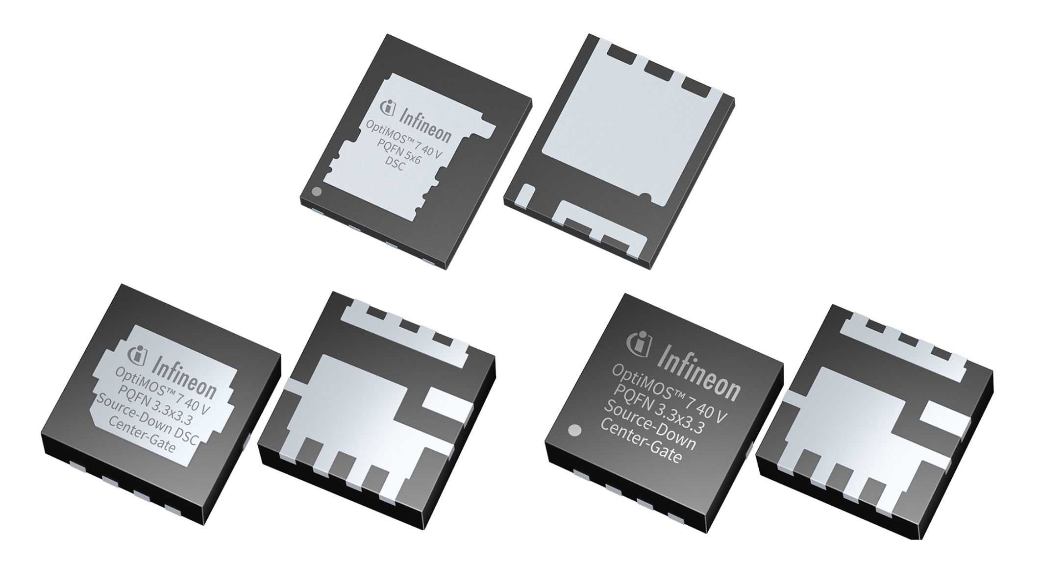
Two devices use a 3.3 × 3.3mm PQFN source-down centre-gate package: the IQE010N04LM7CG and IQE010N04LM7CGSC. The latter adds dual-side cooling, while the former is offered in an overmoulded arrangement. Infineon specifies a maximum RDS(on) of 1.0mΩ at 10V gate-source voltage for both, providing a common conduction specification with different thermal packaging options.
The source-down arrangement changes the physical path through which current and heat pass between the semiconductor and its mounting structure. The centre-gate configuration also affects how the gate connection can be routed in a compact power-stage layout. Parasitic resistance and inductance in conductors and package connections influence switching behaviour, particularly where devices operate at high current and frequency.
Three further devices use 5 × 6mm drain-down PQFN packages with dual-side cooling. The ISCH65N04LM7SC, ISCH69N04LM7SC, and ISC011N04LM7SC have maximum on-state resistances of 0.65mΩ, 0.69mΩ, and 1.1mΩ respectively at 10V gate-source voltage. The differing electrical characteristics and physical dimensions give designers options when matching the transistor to current requirements, cooling arrangements, and available board area.
Infineon rates the MOSFETs for junction temperatures up to 175°C. The rating describes a semiconductor limit, not a target temperature for sustained operation of the surrounding electronics. Actual junction temperature depends on device dissipation, ambient conditions, thermal interfaces, circuit board construction, and the chosen cooling system. A dual-side cooling package provides another route for heat removal, but its benefit depends on the mechanical design of the assembly.
The connection to 800V rack distribution needs a distinction between electrical system levels. A 40V MOSFET cannot directly switch an 800V DC bus; it belongs in a lower-voltage stage downstream of suitable conversion and isolation circuitry. Higher-voltage distribution architectures may alter how energy is routed around a data centre rack, while the final stages still need components that regulate the much lower voltages used by computing electronics.
Existing 48V architectures present related conversion requirements. The voltage applied to any individual transistor depends on the specific circuit rather than the nominal system distribution voltage alone. The suitability of the 40V part must therefore be established from the local switching-node stress, transients, and protection arrangement, including an appropriate electrical design margin.
Infineon’s OptiMOS range already includes devices designed for other priorities, including automotive switching and low-conduction-loss applications. This launch extends the family with components optimised specifically for fast DC-DC conversion rather than repeating the recent automotive MOSFET additions. It also complements earlier reference designs for server power, without being the same product as a complete converter board.
The 40V switching-optimised devices are available in mass production. Integration into customer equipment will require evaluation of switching losses, electromagnetic interference, thermal performance, and package layout under the operating conditions of the intended converter. Those measurements will establish how much of the transistor-level improvement can be realised at the level of the finished power supply.