IN Brief:
- Imec is building a Hokkaido research team of approximately 15 people over five years.
- Planned work includes photonic integrated circuits, electronic-photonic integration, and advanced packaging research.
- The new base supports research collaboration, not a newly announced commercial chip fabrication plant.
imec is establishing a semiconductor and photonics research presence at Hokkaido University in Sapporo, Japan. The Belgian research organisation intends to build a local team of about 15 researchers and engineers over the next five years, linked to its existing activities in Leuven. The initiative is an R&D expansion, not a new commercial chip fabrication plant.
The expansion has the backing of Japan’s Ministry of Economy, Trade and Industry and involves the Leading-edge Semiconductor Technology Center. Research will focus on photonic integrated circuits and devices combining optical and electronic functions, with the stated aim of supporting future advanced semiconductor systems and industry commercialisation programmes.
The Hokkaido programme will connect Japanese research groups and semiconductor businesses with imec’s European R&D facilities. Researchers will work on electronic and photonic devices, including approaches intended to integrate optical links into advanced semiconductor systems. The announcement does not specify a production timetable, a dedicated commercial fabrication line, or a qualified manufacturing process for the new location.
The planned collaborations involve Hokkaido University, Tohoku University, Yokohama National University, the National Institute of Advanced Industrial Science and Technology, and Chitose Institute of Science and Technology. They provide a combination of device research, materials expertise, semiconductor engineering, and academic training. imec intends to coordinate these activities with its wider research network rather than establish a separate organisation limited to one university.
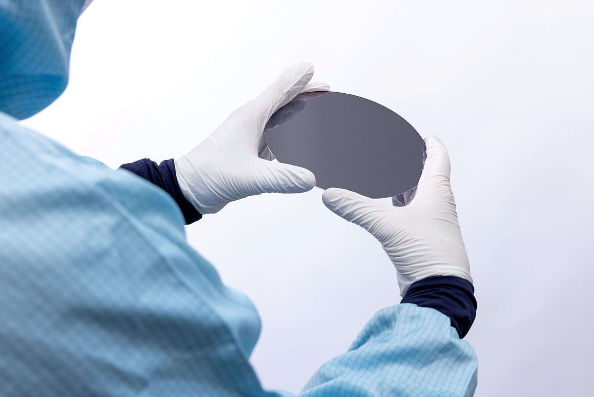
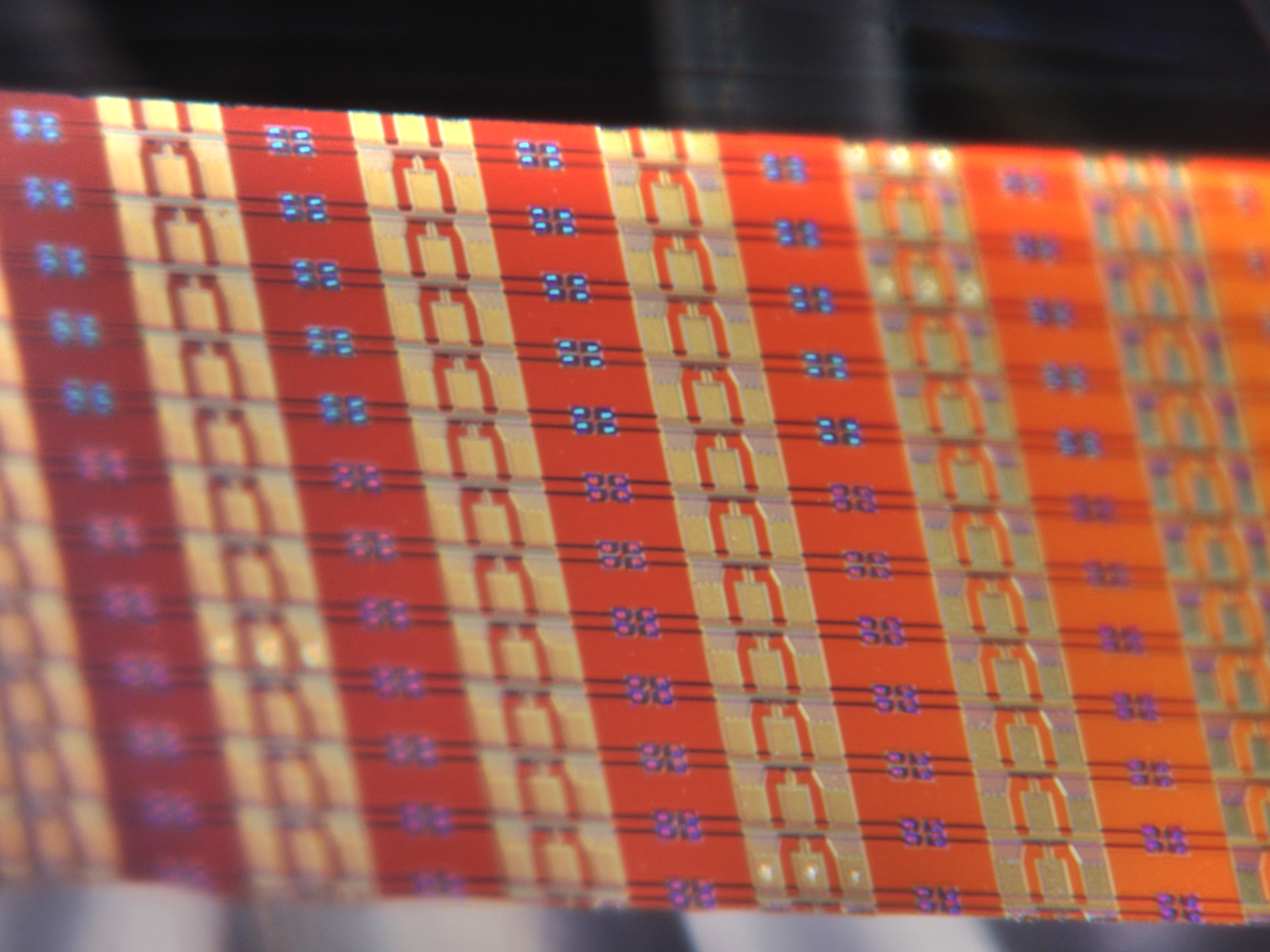
A photonic integrated circuit routes and manipulates light through structures formed on a chip, rather than using only electrical signals within conventional circuitry. Optical links are being investigated for moving data between high-performance processors and other system components, particularly where electrical interconnect losses, bandwidth, and power requirements become limiting factors as data rates rise.
Co-packaged optics places optical communications functions closer to computing or switching components within a shared package or closely integrated assembly. Bringing optics into such systems requires work beyond an individual photonic device: the electrical interfaces, packaging, optical coupling, thermal behaviour, assembly tolerances, and testing methods must operate together. A photonic circuit that performs in isolation does not automatically translate into a practical high-volume packaged system.
Imec’s research programme is intended to address photonic integrated circuits and electronic-photonic integrated circuits, connecting component-level advances with wider system requirements. The institute has not specified a production schedule or announced that any particular process has completed industrial qualification through the new Hokkaido base.
The location also extends an existing relationship. Imec and Hokkaido University signed a letter of intent in November 2024 to explore semiconductor cooperation. Kiyohiro Houkin, President of Hokkaido University, says joint projects involving co-packaged optics in advanced semiconductor packaging and medical AI applications began during 2026, while graduate student training at imec has also started.
An operational research team would extend the relationship beyond the 2024 letter of intent. Imec has named Rapidus among the industry partners whose commercialisation efforts could benefit from the research, but it has not identified the Hokkaido team as a Rapidus production operation. The initially planned staffing level is consistent with a research coordination and development programme rather than a semiconductor manufacturing facility.
Patrick Vandenameele, CEO of imec, linked the initiative to Japanese expertise in semiconductor materials, equipment, and manufacturing. Research across several institutions will still require common interface specifications, repeatable measurements, and packaging methods before an individual device concept can be used in a larger electronic or optical system. None of those later qualification steps is described as completed by the new Hokkaido arrangement.
The next identifiable steps are recruitment for the Hokkaido team and continued work on photonic integrated circuits and electronic-photonic integration. Results from the university collaborations will have to be assessed against device, packaging, and system requirements before any industrial partner can establish a route to commercial deployment.