
IN Brief:
- Lam has started construction of a 120,000ft² R&D laboratory at its Tualatin campus.
- The building is expected to increase the site's cleanroom laboratory space by more than 50%.
- The 2028 opening will provide the first physical milestone in Lam's planned $3 billion-plus global laboratory expansion.
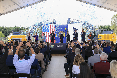
Lam Research has started construction of a 120,000ft² semiconductor R&D laboratory at its Tualatin campus in Oregon, putting the first site-specific build behind a planned investment of more than $3 billion across its global laboratory network. The facility is expected to open in 2028.
The new building is expected to increase cleanroom laboratory space at the Tualatin R&D centre by more than 50%. Lam plans specialised capability for deposition and etch process development, materials science, and hardware validation, with customers able to work alongside its engineers from early process concepts through preparation for deployment in their own fabs.
This is laboratory capacity rather than additional wafer-production capacity. Lam supplies wafer-fabrication equipment and process technology, so the output will be experiments, process recipes, hardware validation, and qualified manufacturing techniques rather than a published number of wafers per month. The work nevertheless sits directly upstream of fab ramps because new device structures depend on equipment and processes being qualified before production volumes rise.
The development burden has increased as leading logic, advanced memory, and heterogeneous integration use more complex three-dimensional structures and material combinations. Deposition and etch steps interact with cleaning, metrology, lithography, thermal budgets, and packaging requirements, while small changes intended to improve one feature can create defects or yield losses elsewhere in the sequence.
More cleanroom space gives engineering teams room to run additional experiments in parallel, but experiment count alone is not the target. Useful R&D capacity has to produce repeatable process windows, stable hardware, credible metrology, and enough data for customers to decide whether a technique can survive high-volume manufacturing. Tool availability, chamber matching, maintenance, and materials control become part of the result once development moves beyond a laboratory demonstration.
Lam announced the wider programme earlier in August, setting out plans to spend more than $3 billion over five years and increase experiment capacity across its laboratory network by more than 50%. That programme was covered in the company’s global laboratory expansion plan. The Tualatin groundbreaking now identifies where part of that capital will become physical cleanroom and engineering infrastructure.
Oregon places the new facility inside an established semiconductor cluster and close to major customers. Senior representatives from Intel and Micron joined the groundbreaking, reflecting the collaboration Lam expects the laboratory to support. Proximity can shorten the practical cycle around wafers, hardware, and engineering teams when process changes have to be evaluated repeatedly before qualification.
The project also carries a sizeable construction and employment programme. A third-party assessment using inputs supplied by Lam estimates about 900 jobs and $500 million in economic output over the three-year construction period. Once completed, the wider campus expansion is projected to create more than 400 new Lam jobs, take the number of jobs supported by the company across Oregon above 11,000, and lift its annual economic contribution in the state above $1.8 billion.
Those figures are projections rather than delivered outcomes, and the laboratory still has a two-year construction and fit-out path before its planned 2028 opening. Semiconductor R&D buildings also need more than conventional construction completion: cleanrooms, utilities, process tools, contamination controls, software, safety systems, and measurement equipment have to be installed and qualified before engineers can use the space productively.
The Tualatin project gives the wider investment programme a concrete first milestone without changing its underlying purpose. Lam is adding development infrastructure where new materials and process steps are turned into manufacturing methods that customers can qualify. After 2028, the relevant measure will be whether the extra cleanroom and tool capacity shortens the path from experimental process to stable fab deployment as device structures become harder to manufacture.
