IN Brief:
- Samsung’s zHBM concept places high-bandwidth memory directly above an AI accelerator.
- The company has published projected density, efficiency, and performance improvements but no production timetable.
- Samsung also presented zNAND-O and 400-plus-layer V10 Bonding V-NAND for future AI storage systems.
Samsung Electronics has presented concept models for vertically integrated high-bandwidth memory and NAND architectures, moving memory above or around processing devices rather than treating it as a separate package-level component.
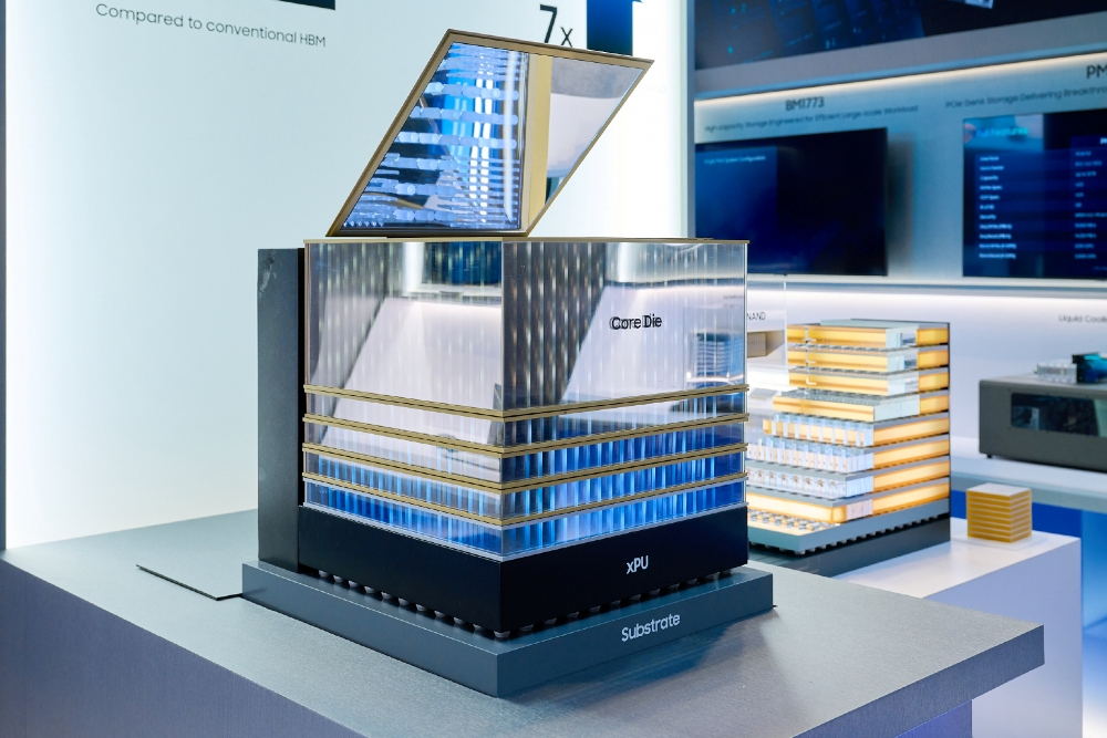
The zHBM concept places high-bandwidth memory directly above an artificial intelligence accelerator. Current HBM packages normally position several stacked DRAM devices beside the processor on an interposer or advanced substrate. Samsung’s proposed arrangement shortens the physical data path and could increase the amount of memory that fits within a given package footprint.
Samsung says a future interface built around zHBM could provide approximately eight times the performance of HBM5, more than ten times its memory density, three times its energy efficiency, and less than half its thermal resistance. Those figures are design targets attached to a concept model rather than measurements from a qualified production device.
The company also proposes an interlayer between the memory and accelerator that could carry customer-specific intellectual property. That approach would allow memory, logic, and specialised functions to be co-designed within one vertical structure, but it would also tie package development more closely to a particular processor and customer programme.
Vertical integration addresses several limits in conventional side-by-side packaging. HBM interfaces already move large amounts of data over a wide bus, but increasing stack capacity and pin speed places pressure on interposer routing, package area, signal integrity, and power delivery. Shorter vertical connections could reduce some of that burden while giving designers more freedom around the package perimeter.
Thermal engineering is the obvious complication. AI accelerators dissipate substantial heat, while DRAM performance and retention are temperature-sensitive. Stacking memory directly above the processor concentrates both devices in one heat path. Samsung’s claim of lower thermal resistance implies a bonding and cooling strategy designed around that problem, but it has not published layer temperatures, cooling requirements, package dimensions, or sustained workload data.
Manufacturing yield is equally important. A package that combines several memory dies, an interlayer, and an expensive accelerator can lose significant value if one element fails late in assembly. Known-good-die testing, bonding alignment, warpage, through-layer interconnects, repair strategy, and final test access will affect whether the density advantage can be produced economically.
Samsung also introduced zNAND-O, a V-NAND-based architecture being developed in four-layer and eight-layer versions. It is intended for edge AI systems requiring lower latency, greater input/output performance, and high storage density. The company has not disclosed endurance, interface, controller, capacity, or production specifications.
Edge systems often sit between DRAM and conventional storage constraints. DRAM provides low latency but is relatively expensive and power hungry at large capacities, while NAND offers density but requires controllers, error correction, and block-management software. A vertically integrated NAND design positioned close to compute could reduce data movement, provided its latency and endurance suit the workload.
The third element of Samsung’s presentation was V10 Bonding V-NAND with more than 400 layers. The company says wafer bonding increases memory density by about 58% over its V9 generation and improves read, write, and input/output performance. Bonding allows memory-cell and peripheral-circuit structures to be fabricated separately before joining, creating another route to higher layer counts.
Separating those fabrication steps can allow each wafer to use a process better suited to its function, but it introduces bonding yield, alignment, and interface-control requirements. As layer counts rise, manufacturers must also control channel formation, etch uniformity, wafer bow, and electrical variation across a much deeper memory structure.
Samsung’s zHBM and zNAND-O disclosures are therefore architectural signals rather than product launches. No interface standard, customer qualification, sampling date, mass-production timetable, or commercial specification has been published. Their value lies in showing that memory development is moving beyond faster pins and taller stacks towards co-designed systems that combine logic, DRAM, NAND, bonding, and thermal management.
The next evidence will need to come from test silicon and package data. Bandwidth, power, cooling, yield, repairability, and manufacturing cost will determine whether vertical processor-memory integration becomes a broadly supported platform or remains restricted to expensive customer-specific accelerators.