IN Brief:
- UMC and AP Memory are combining foundry technology and silicon capacitor designs for advanced semiconductor power networks.
- AP Memory's S-SiCap Gen2D discrete capacitor designs completed tape-out and initial functional validation during the third quarter of 2026.
- Package-level performance and reliability testing must follow before claims about commercial operating performance or qualification can be made.
United Microelectronics Corporation (UMC) and AP Memory have agreed to develop silicon capacitors for advanced semiconductor packaging, combining the foundry’s deep trench capacitor manufacturing technology with AP Memory’s component design and integration work. The partners are targeting the power delivery networks used by AI accelerators and high-performance computing devices.
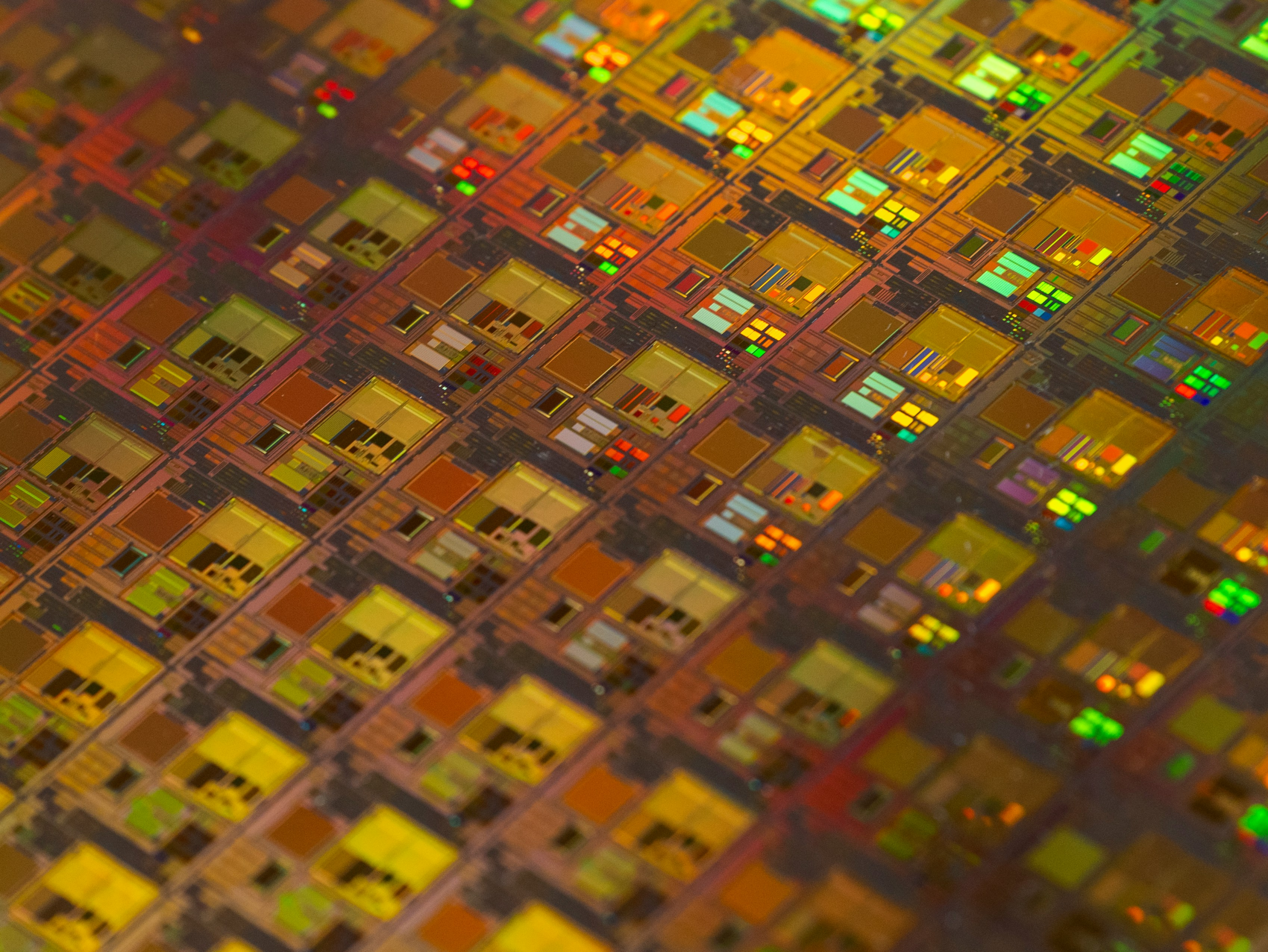
The companies have reported an initial manufacturing milestone rather than a finished, qualified product. AP Memory’s S-SiCap Gen2D discrete silicon capacitor designs completed tape-out and initial functional validation during the third quarter of 2026. The next step is system-level performance and reliability testing after the devices have been incorporated into substrate packages.
As power demands rise in advanced processors, the electrical connection between voltage regulation equipment and the computing die becomes increasingly important. High current and rapid changes in load can produce fluctuations at the point where a chip receives power. The resistance and inductance of conductors, package connections, and other structures affect how quickly the supply network can respond.
Decoupling capacitors provide a local store of electrical charge that can supply or absorb current over short intervals. Their effectiveness depends on capacitance, frequency-dependent behaviour, and the impedance of the path connecting them to the load. A capacitor placed on a motherboard may be electrically distant from a die even when the physical separation appears small.
Advanced packages contain substrates, interposers, and dense networks of electrical connections. Integrating capacitors into those structures can shorten part of the path between stored charge and the circuits needing it. The objective is to improve local power integrity and support voltage regulation during rapid load changes, although any benefit must be measured within the actual package and power distribution architecture.
UMC’s deep trench capacitor technology increases the electrode area available inside a silicon component by forming narrow, deep features rather than relying only on planar structures. This approach can create high capacitance density in a compact footprint. It also requires precise manufacturing of the trench geometry, dielectric, and conductive layers so that electrical properties remain consistent across devices and wafers.
The partnership assigns complementary roles to the two companies. UMC provides the foundry process and scalable wafer manufacturing capabilities, while AP Memory contributes its S-SiCap designs and system integration expertise. Moving from a design tape-out to initial wafer validation establishes a basis for further development, but does not demonstrate that a capacitor will remain reliable when embedded in a complete semiconductor package.
Package integration introduces additional variables. Connections must meet the electrical requirements of the power network, while dielectric breakdown, leakage current, and the capacitor’s behaviour over voltage and temperature need to be assessed. Mechanical stress and differences in thermal expansion can also affect embedded structures during assembly and subsequent operation.
The partners say the forthcoming testing will cover a range of capacitance and operating voltage requirements in substrate packages. Their statement does not specify an achieved capacitance density, a quantified reduction in supply noise, or a performance improvement measured on a commercial AI processor. Those figures cannot be inferred simply from the use of deep trenches or proximity to the die.
Several physical arrangements are being considered. Discrete silicon capacitors can be positioned within the wider package architecture, while capacitor-embedded interposers would incorporate the charge-storage function into structures connecting semiconductor elements. Landside capacitors provide another arrangement, located on the underside of a package substrate. Each option creates different electrical, thermal, manufacturing, and space constraints.
The preferred arrangement depends on the chip’s operating voltage and transient current demand, the package geometry, and the space allocated to other connections. Capacitors with useful high-frequency behaviour may address only part of the power distribution problem, because voltage regulators, conductors, and larger energy storage elements must still supply sustained current. Effective power delivery requires these components to work as a coordinated network.
UMC’s published roadmap extends beyond discrete capacitors to embedded silicon capacitors and active devices, including internal voltage regulators. The foundry is also investing in additional manufacturing capacity intended to support power delivery components and heterogeneous semiconductor integration. The announcement does not give a value for that investment or a production schedule specific to the AP Memory designs.
The collaboration gives AP Memory a foundry route for its capacitor technology and gives UMC a design partner for advanced packaging applications. Whether it progresses into customer products will depend on the planned package-level electrical and reliability results, subsequent qualification requirements, and manufacturing economics. For now, the confirmed achievement is an initial tape-out and functional validation, with full system performance still to be established.