IN Brief:
- VersaXRM 5 Insight combines microCT-style overview imaging and higher-resolution X-ray microscopy in one platform.
- ZEN navx, Volume Scout, FAST mode, and deep-learning reconstruction support guided overview-to-detail workflows.
- Semiconductor applications include locating buried interconnects, package defects, and reliability risks before destructive cross-sectioning.
ZEISS has introduced VersaXRM 5 Insight, a hybrid 3D X-ray microscope combining microCT-style overview imaging with higher-resolution X-ray microscopy in one workflow. The platform targets semiconductor, electronics, materials, battery, and research laboratories that need to move from inspection of a complete sample to detailed internal analysis without cutting it apart first.
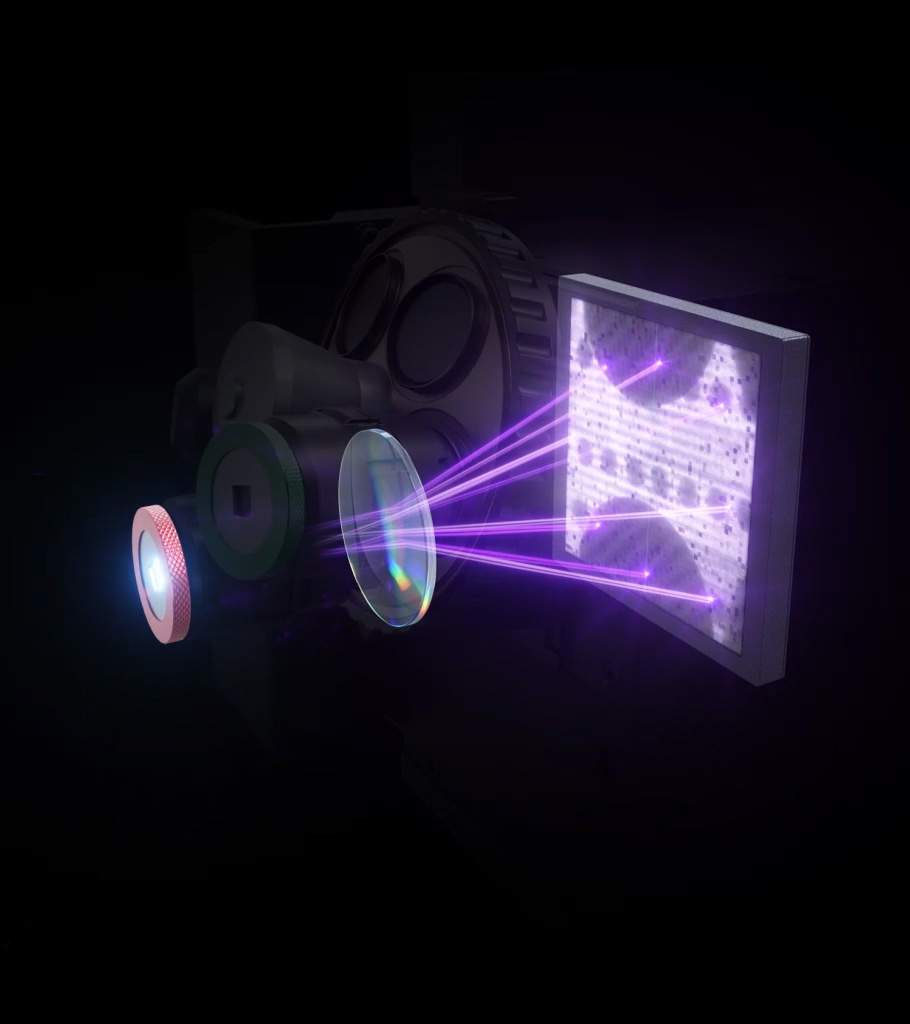
The system combines flat-panel overview imaging with ZEISS Resolution at a Distance objective-based X-ray microscopy. Users can scan a complete component, select a region of interest inside the reconstructed volume, and then move to higher-resolution imaging while retaining its position within the larger sample.
Keeping those stages on one platform reduces the need to transfer a sample between instruments or repeatedly remount it as the investigation moves to a smaller feature. That becomes useful where an internal defect is difficult to locate from its external position or where destructive preparation could remove the surrounding evidence needed to understand the failure.
ZEN navx provides the navigation layer. Parameter Guidance supports scan setup, while Volume Scout allows regions of interest to be selected within three-dimensional data. FAST mode handles rapid overview acquisition, and the same software environment carries the operator towards more detailed imaging.
ZEISS has also integrated several reconstruction tools. DeepRecon Pro uses deep-learning reconstruction to improve contrast and edge definition while reducing noise; DeepScout is intended to increase effective resolution across larger overview scans; and other algorithms address multi-material artefacts, phase contrast, and the trade-off between image quality and acquisition time.
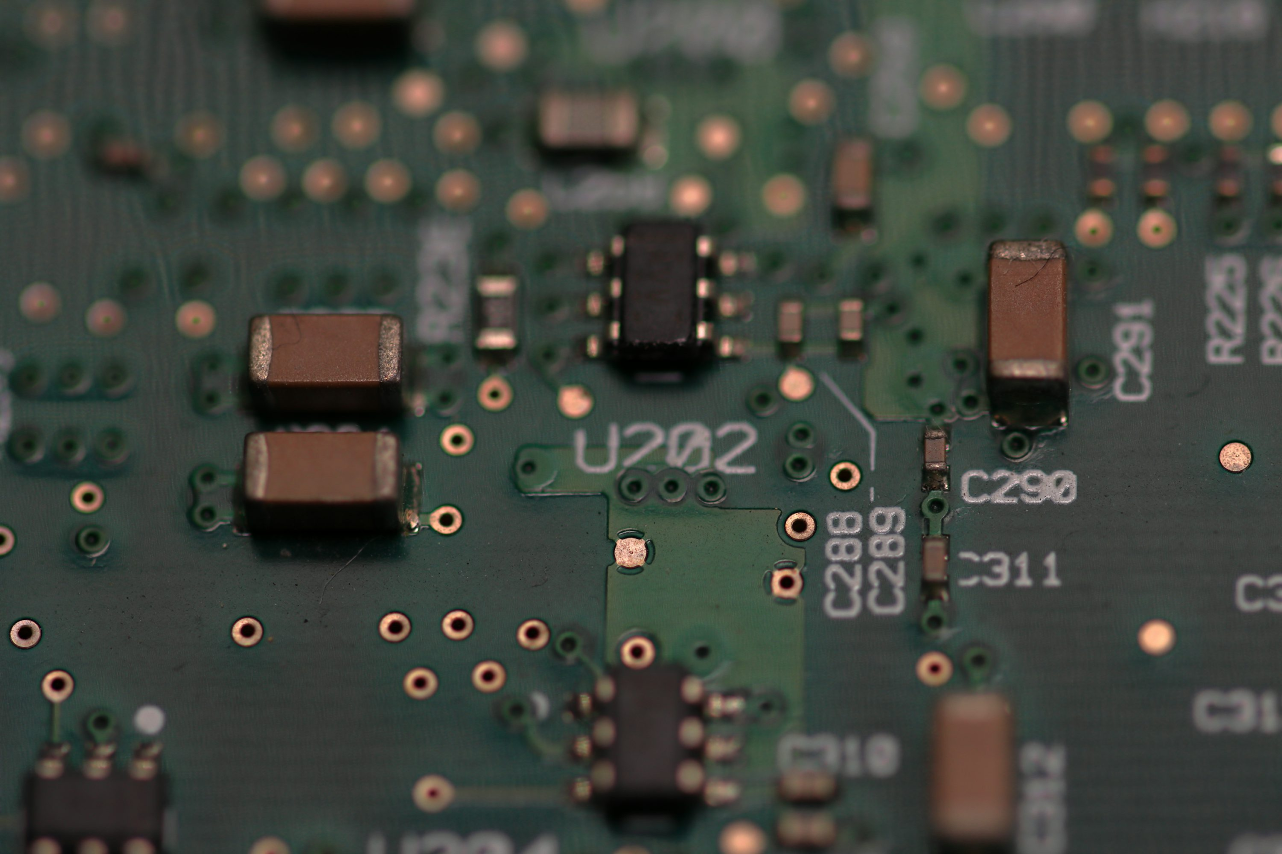
Electronics and semiconductor packaging provide a direct application for that combination. ZEISS demonstrates the platform on structures including C4 bumps and microbumps inside a 5G modem package, where the initial requirement is to find the relevant internal area before spending high-resolution scan time on an individual interface or suspected defect.
That workflow becomes more demanding as packaging moves towards chiplets, stacked memory, heterogeneous integration, and denser vertical interconnects. A package can contain several materials, dies, redistribution layers, solder structures, and bonding interfaces, creating failure sites at very different physical scales.
Conventional microCT remains useful for rapid volumetric inspection, while X-ray microscopy provides finer internal detail where the defect demands it. Combining the two does not remove the trade-off between field of view, acquisition time, and resolution, but it allows the operator to make that trade-off without losing the coordinates established during the wider scan.
The system can also reduce unnecessary destructive analysis. Cross-sectioning remains essential when physical or chemical examination of an interface is required, but selecting the section from prior 3D data improves the chance of cutting through the actual defect rather than an adjacent region. The intact sample can also be retained for other investigations when the X-ray data provides sufficient evidence on its own.
VersaXRM 5 Insight arrives alongside wider ZEISS investment in semiconductor metrology and optical production. The company has been expanding German capacity for semiconductor optics and metrology systems used around advanced manufacturing and packaging, reflecting growing inspection requirements across both wafer processing and downstream assembly.
The new platform is positioned below the highest-performance members of the VersaXRM range rather than as a replacement for every CT or XRM system. ZEISS describes it as an entry into true X-ray microscopy with a workflow optimised around moving from broad sample context to selected internal detail.
Laboratories will ultimately assess the system through achievable resolution at practical working distances, scan speed, reconstruction time, performance on dense multi-material structures, and the repeatability with which operators can return to an identified internal feature. Shared facilities also have to balance sophisticated imaging capability against training time and instrument utilisation.
VersaXRM 5 Insight addresses that balance by putting overview imaging, 3D navigation, high-resolution acquisition, and reconstruction into the same environment. In electronics failure analysis, where the first problem is frequently finding the defect before characterising it, that workflow can be as important as the maximum resolution claimed for the final scan.