IN Brief:
- Keysight Multiphysics integrates structural analysis into the electronic product-development workflow.
- Guided templates automate mesh creation, contacts, materials, and compliance load cases.
- The first application supports drop, shock, and vibration assessment against MIL-STD, IEC, and JEDEC requirements.
Keysight Technologies has introduced a multiphysics design and verification environment whose first application brings drop, shock, and vibration analysis into the electronic product-development workflow.
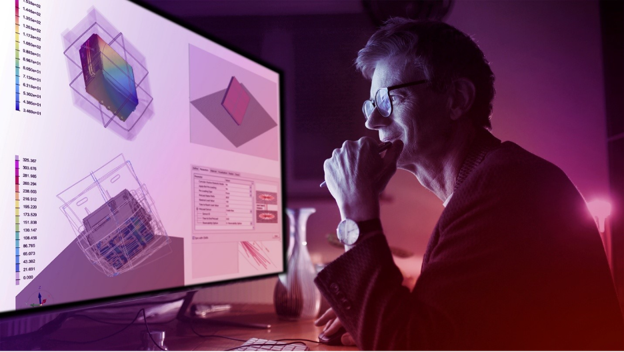
Keysight Multiphysics is intended to expose structural reliability problems before a physical prototype is built. Guided templates automate model setup and provide preconfigured load cases for compliance work involving MIL-STD, IEC, and JEDEC shock, vibration, and drop requirements.
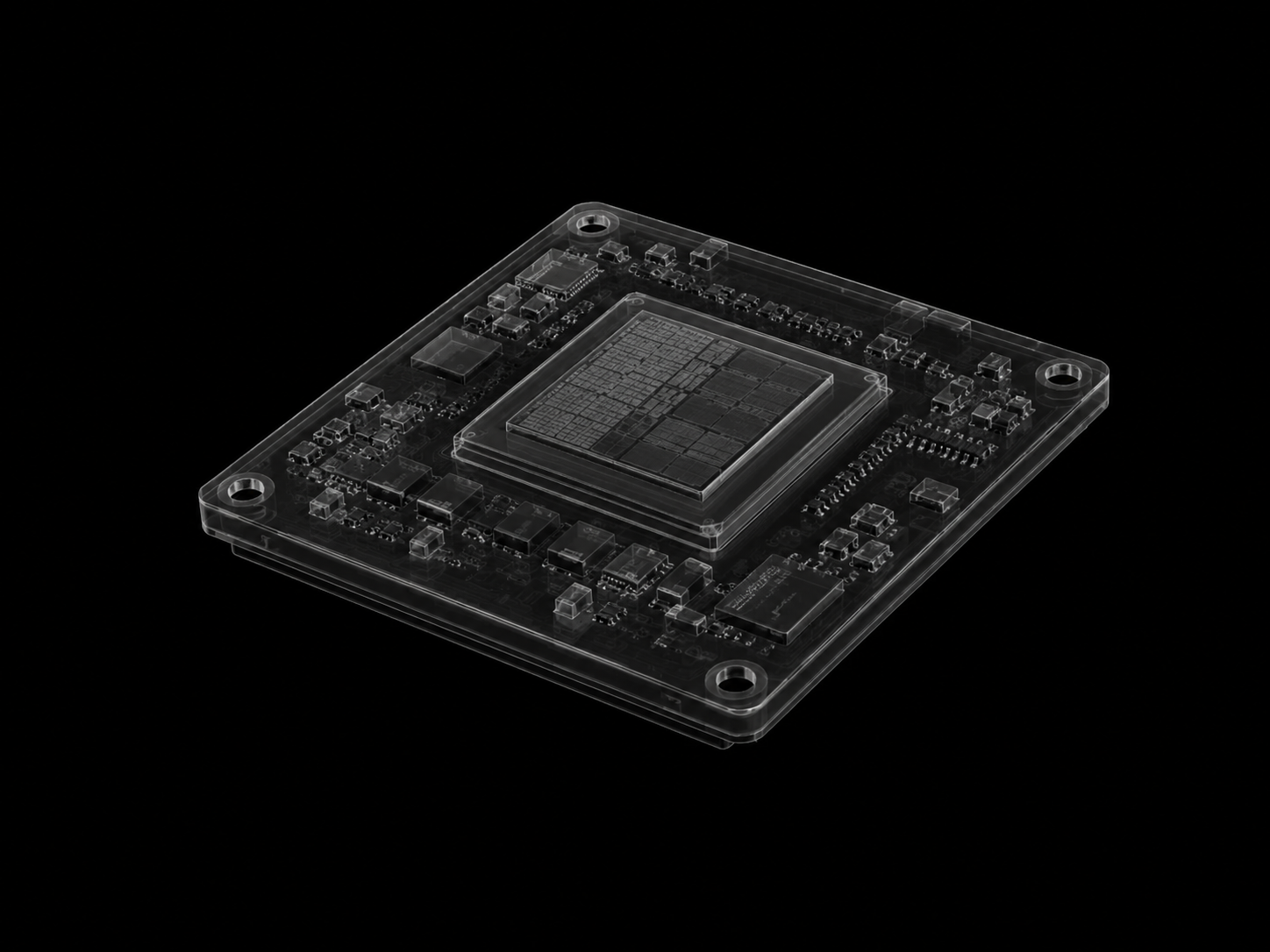
The software addresses assemblies containing enclosures, printed circuit boards, connectors, fasteners, and internal components. An electronics-specific material database supplies mechanical properties for commonly used materials, reducing the information that must be assembled before analysis can begin.
Automated functions cover mesh generation, contact definition, material assignment, screws, weld connections, and other model relationships that traditionally require specialist finite-element-analysis experience. Completed workflows can be stored as templates and reapplied to product variants, preserving modelling choices across a family of related designs.
Available outputs include stress, strain, acceleration, displacement, and PCB curvature. Custom shock and vibration profiles can also be created where an internal qualification method or installed operating environment differs from a standardised test profile.
Keysight specifies that a drop analysis can be completed in about one hour when suitable high-performance computing resources are available. The solver can scale across hundreds of CPUs, although calculation time will vary with model size, mesh density, contact behaviour, material representation, and the duration of the simulated event.
Electronic reliability has traditionally been divided between electrical design, thermal analysis, mechanical engineering, and physical compliance testing. Those boundaries are increasingly difficult to maintain as products become smaller, more powerful, and more densely assembled.
A mechanical impact can flex a PCB, crack a solder joint, damage a ceramic component, loosen a connector, or change contact pressure at a thermal interface. The electrical fault may appear only after repeated vibration or a later temperature cycle, making the original structural cause difficult to isolate.
Thermal behaviour changes the same problem because materials expand at different rates, solder and polymers alter stiffness with temperature, and hot components create local gradients across the board and enclosure. An assembly that survives a room-temperature drop test may respond differently after thermal ageing or near an operating-temperature limit.
Physical prototypes remain necessary for correlation and qualification, but finding a structural weakness after tooling has been committed is expensive. Enclosure geometry, board mounting, component placement, connector support, and fastener design may all need to change together, with corresponding effects on EMC, cooling, industrial design, and manufacturing.
Virtual analysis has greatest value while those features remain adjustable. Board supports, enclosure ribs, component locations, and damping methods can be compared before another moulded part or assembled prototype is ordered, while predicted strain and acceleration can guide the placement of gauges and sensors during subsequent laboratory testing.
Automation lowers the barrier to an initial study without removing engineering judgement. Results remain dependent on geometry, boundary conditions, material models, contacts, damping assumptions, and applied loads, and a visually convincing stress map can still be misleading when the assembly has been constrained in a way that does not represent the physical product.
Correlation therefore remains part of the workflow. Measurements from instrumented drop and vibration tests can be compared with predicted acceleration, displacement, and board strain, allowing the model to be adjusted before it is reused for another variant or compliance profile.
Multiphysics analysis is also moving closer to PCB and package implementation elsewhere in the design chain. Cadence’s AuraStack environment coordinates electrical, thermal, and mechanical analysis around board and advanced-package development, while Keysight’s first application concentrates on guided structural reliability and compliance.
Wider access creates a governance requirement because organisations need to define which simulations may be performed through approved templates, which assumptions can be changed, how models are reviewed, and when specialist intervention is required. Reusable workflows improve consistency only when their inputs, version history, and limitations are controlled.
Standards-based templates can accelerate preparation for regulatory testing, but simulation does not replace certification. Laboratory fixtures, mounting conditions, manufacturing tolerances, cable behaviour, component variability, and accumulated ageing still influence the physical result and must be represented by an appropriate test programme.
Keysight is beginning with structural analysis before extending the environment across additional interacting physical domains. The first release addresses a common source of late redesign: an electronically functional product that cannot reliably survive its mechanical environment, despite having progressed far enough for changes to affect the board, enclosure, tooling, and manufacturing process together.