IN Brief:
- Photon Bridge has raised €10 million in a round co-led by Amadeus APEX Technology Fund and 360 Capital.
- The company combines lower-power semiconductor lasers and targets output of up to 40mW per wavelength per fibre.
- Customer samples are planned for 2027, with preparations for volume manufacturing from 2028.
Photon Bridge has raised €10 million to develop multi-wavelength semiconductor laser sources for optical connections in AI computing infrastructure. The Eindhoven company is concentrating on how large numbers of laser devices could be manufactured consistently as optical links are brought closer to the processors and switching equipment that exchange data across computing clusters.
The financing was co-led by the Amadeus APEX Technology Fund and 360 Capital. Existing investors Innovation Industries, Faber and the Brabant Development Agency, known as BOM, also participated. The money will support product development, customer qualification and recruitment. Photon Bridge plans to deliver its first customer samples in 2027 and prepare for volume manufacturing from 2028; neither milestone represents a product already being shipped at commercial scale.
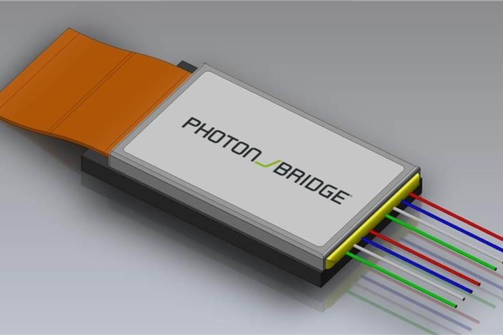
Its architecture combines and multiplexes light from multiple lower-power semiconductor lasers, instead of depending on a smaller number of individual lasers producing progressively higher optical power. Photon Bridge says distributing the required output in this way can reduce the sensitivity of each laser to manufacturing defects and improve production yield. These are supplier-reported manufacturing advantages, with customer qualification still to establish their performance in finished products.
The company is designing the platform for high wavelength counts, with up to 40mW of optical power per wavelength per fibre. That figure is a stated platform design capability, rather than a measured specification for a particular customer-qualified production module. Photon Bridge also wants its manufacturing approach to operate across multiple indium phosphide foundries, reducing dependence on a single fabrication route as production volumes increase.
Indium phosphide is an established material for active photonic components that generate light for communications links. Its manufacturing requirements differ from those of the silicon electronic circuits handling computation and data switching. Building complete optical assemblies therefore involves combining components produced with different material systems, alongside packaging, electrical connections, optical coupling and testing. The announcement identifies broader foundry compatibility as an objective but does not document production yields achieved across several factories.
Wavelength multiplexing enables light at different wavelengths to travel through a common optical path. The technique can support multiple communication channels over a fibre, provided the system includes suitable modulation, wavelength management and receiving equipment. Delivering more wavelengths from a single source assembly may help increase channel density, but the useful system capacity also depends on optical losses, signal quality and the architecture of the interconnect.
Large AI installations require traffic to move between computing accelerators, memory and network switches. As the number of connected processors increases, the bandwidth and energy required for those exchanges become important equipment constraints. Electrical and optical links have different properties over distance, with optical systems introducing their own power budgets, connector tolerances and requirements for generating and distributing light.
Co-packaged optics places optical interfaces close to high-performance electronic chips, reducing some electrical interconnect distances while increasing demands on assembly and maintenance. The lasers supplying those interfaces may be located outside the main electronic package, with light routed into it through fibres. Such arrangements can ease some thermal constraints on the light sources, although loss along the path and alignment at optical connections still influence the total power available.
Photon Bridge’s strategy centres on the laser supply problem rather than a completed replacement for copper interconnects. The company cites an Omdia forecast of more than 20 million data centre AI accelerators shipping annually by 2028 as an indication of potential scale. That is an industry forecast used in its commercial case, not a confirmed sales forecast for Photon Bridge or evidence of purchase orders for its technology.
Manufacturing yield becomes particularly important when large numbers of optical sources must meet defined requirements for output, wavelength and reliability. Even where individual devices perform adequately in laboratory tests, variations between batches can affect usable production volumes. The company’s planned customer qualification process should help establish whether its distributed laser approach meets practical expectations for optical output, integration and repeatability.
Photon Bridge previously operated as Photon IP and has also announced collaborations involving photonic fabrication and external laser-source packaging. The latest funding does not specify a factory opening date, commercial shipment volume or named customer commitments. Its next declared milestones are samples in 2027 and manufacturing preparations beginning in 2028, leaving the engineering and commercial performance of the proposed architecture to be demonstrated through qualification.