IN Brief:
- ASML is examining how to produce more than 110 low-NA EUV systems in 2028.
- JPMorgan says EUV assembly speed, rather than component supply, is the current production constraint.
- High-NA adoption is expected to grow while established low-NA EUV remains central to advanced-node manufacturing.
ASML is examining how it could raise low-NA EUV production to more than 110 systems in 2028 as semiconductor manufacturers continue to expand advanced logic and memory capacity. JPMorgan analysts reported the figure after meeting the Dutch lithography company’s chief financial officer.
ASML had already set the direction in its second-quarter results. The company said its 2026 low-NA EUV capacity is around 65 systems and that it plans to add roughly 30% for 2027 while investigating a further 30% increase for 2028. Production above 110 systems would extend that capacity programme as orders move further into the decade.
JPMorgan says ASML is nearly sold out for 2027 and that most new EUV orders are now for 2028 delivery. The analysts identified system assembly speed, rather than the component supply chain, as the principal constraint on higher output.
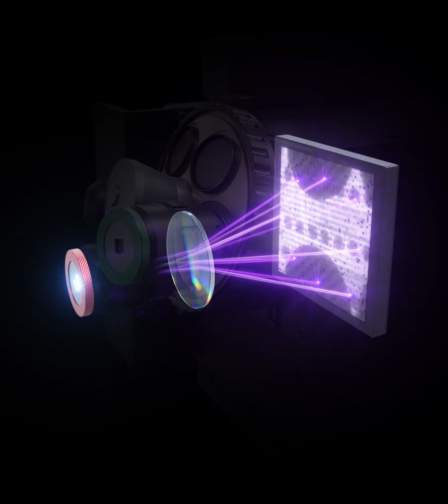
That bottleneck reflects the construction of an EUV scanner. Each system combines a laser-produced plasma light source, vacuum architecture, multilayer reflective optics, wafer and reticle stages, metrology, control electronics, and software. Increasing production therefore requires assembly capacity, specialist labour, calibration equipment, factory space, supplier readiness, and sufficient test throughput to rise together.
ASML reported €9.3 billion of second-quarter net sales and €2.9 billion of net income, with AI-related investment continuing to strengthen customer plans for advanced logic and memory. The company said its order momentum during the first half of 2026 had improved visibility into longer-term demand across its product portfolio.
EUV demand is being driven by both wafer capacity and the number of lithography steps required per device. More EUV layers can increase scanner requirements even before total wafer starts rise, particularly in leading logic and memory processes where patterning complexity continues to increase.
The capacity expansion also overlaps with the industry’s move towards High-NA EUV. The newer platform raises numerical aperture from 0.33 to 0.55 to extend single-exposure resolution, but established low-NA systems will continue to process a much wider range of production layers. A fab introducing High-NA therefore still requires substantial low-NA EUV and DUV capacity around it.
Samsung is among the manufacturers preparing for that transition, with High-NA EUV planned for future DRAM high-volume production from 2028. The timing places new High-NA installations alongside continued expansion of the 0.33-NA fleet rather than replacing it immediately.
Manufacturing more scanners also creates a field-support burden after delivery. EUV equipment has to be installed, qualified, maintained, upgraded, and supplied with replacement modules across fabs operating continuously. Rapid growth in the installed base therefore increases demand on service engineering and logistics as well as on final assembly in the Netherlands.
ASML is planning similar expansion in DUV immersion equipment. Its July results indicated a 30% increase in 2027 capacity from a 2026 base of around 130 immersion systems, with another potential 30% increase being investigated for 2028. Advanced-node capacity consequently places pressure across several lithography classes rather than on EUV alone.
The figure of more than 110 EUV systems is not yet a formal production commitment. ASML has confirmed the underlying 2028 capacity investigation, while the numerical estimate comes from JPMorgan’s meeting with management. Orders, customer fab schedules, supplier readiness, and ASML’s own ability to shorten assembly cycles will determine where actual output lands.
For the semiconductor equipment chain, the shift in constraint is notable. The question is moving from whether suppliers can provide enough parts towards how quickly an extremely complex machine can be assembled, aligned, tested, and accepted without compromising the precision expected from production lithography.
ASML’s 2028 plan will therefore be judged as a manufacturing programme as much as a demand forecast. Advanced logic, AI accelerators, and HBM may be creating the orders, but fulfilling them depends on converting a highly specialised production process into a higher-throughput one without making the machine itself any less exacting.