
Category: Electronics
-

Micron will finance expanded semiconductor materials processing in New York. Its agreement with Indium Corporation supports refining and high-purity manufacturing at the company’s Rome facility, alongside a planned long-term supply arrangement for advanced memory production.
-

The Advanced Photonics Coalition has published five optical manufacturing documents. They cover co-packaged optics, silicon photonics testing and fabrication, and four-core fibre interfaces, with the aim of improving component interoperability and manufacturing repeatability.
-

Samsung Electro-Mechanics has secured a substrate supply agreement with NVIDIA. Existing Korean ABF capacity will support initial deliveries, while planned facilities and upgrades at Sejong and Busan will expand manufacturing for AI processors and networking chips.
-
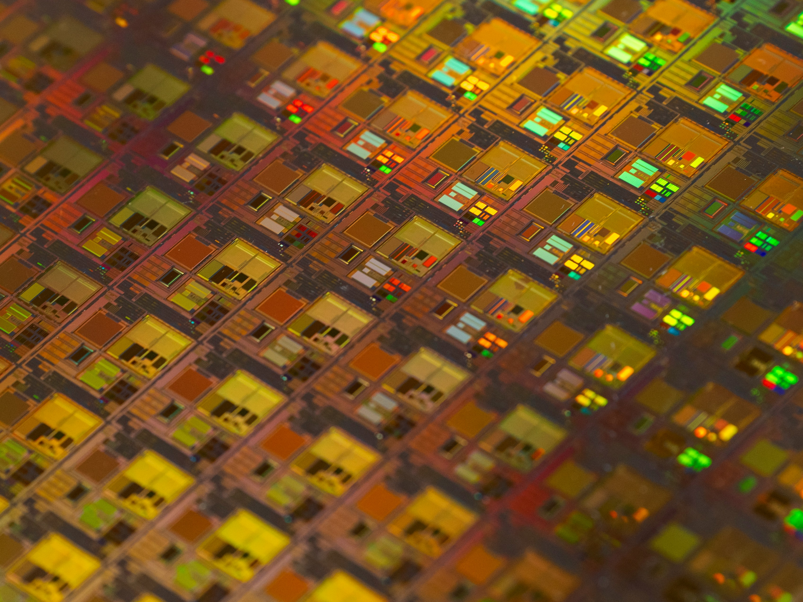
UMC and AP Memory are developing advanced silicon capacitor technology. Their partnership combines deep trench manufacturing and S-SiCap designs for AI processor packages; Gen2D tape-out and initial functional validation are complete, with package-level reliability testing next.
-
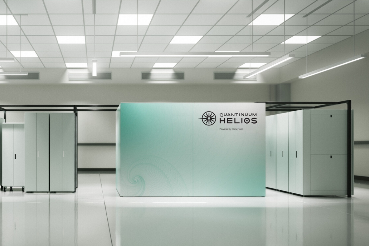
Quantinuum reports improved logical memory protection on its Helios computer. Its distance-seven colour-code result produced 99.9995% fidelity per correction cycle; this is not an end-to-end algorithm success rate.
-
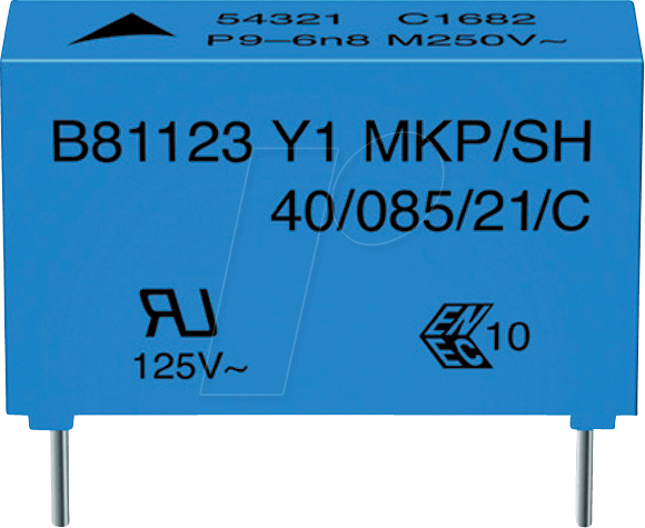
TDK has introduced compact Y1 capacitors for interference suppression applications. The B3201 series supports 500 V AC operation and temperatures up to 125°C, subject to voltage derating and a defined elevated-temperature duration limit.
-
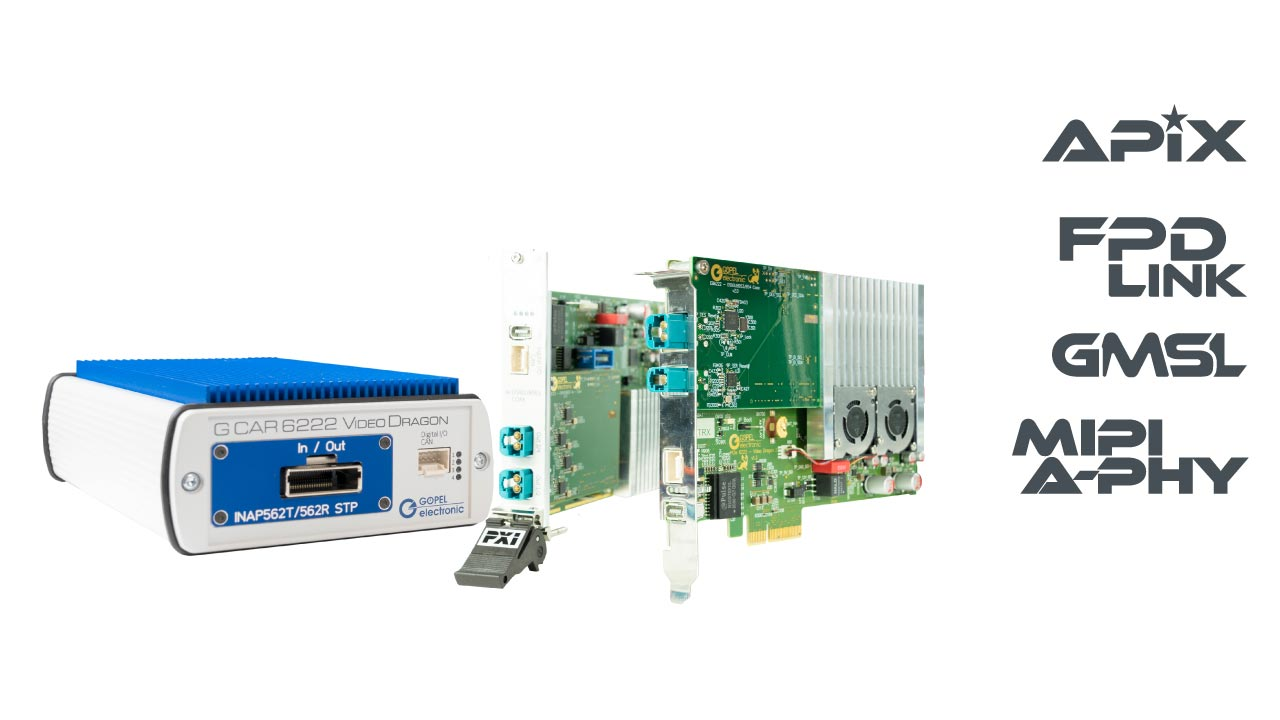
GÖPEL has added ASA-Motion Link support to its Video Dragon. The modular test platform captures and generates video streams for automotive cameras and displays, with standalone and computer-integrated hardware options.
-
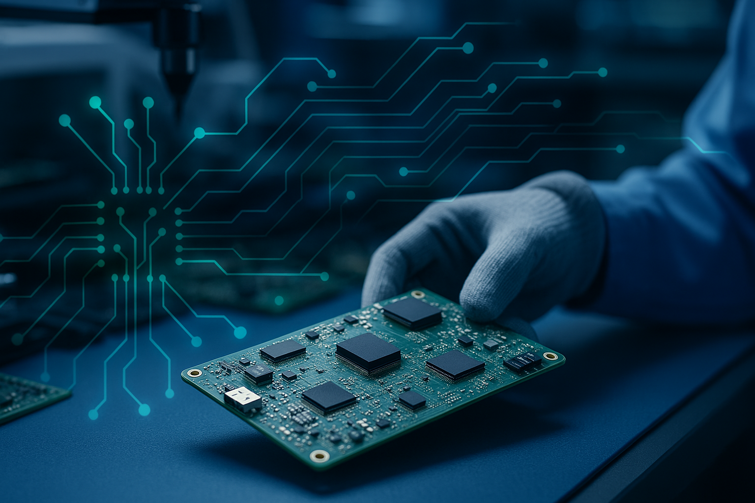
Zuken has extended automation throughout its CR-8000 PCB design platform. The 2026 release introduces schematic routing, placement analysis, locally managed design reuse, EMC checks, and improved routing controls for complex electronics.
-
Socionext is applying Cadence agents to advanced semiconductor physical design. The companies are integrating proprietary engineering knowledge with InnoStack workflows for a large 3 nm SoC; the projected fivefold productivity gain remains unverified.
-
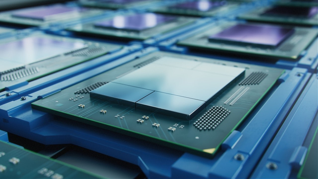
Siemens is automating electrothermal design across advanced semiconductor packaging workflows. An NVIDIA-supported agent coordinates seven EDA tools and nine stages; Siemens reports separate benchmark reductions in engineering effort and setup time.