
Category: Design engineering
-

French researchers have combined memristors and SMTJs for hardware optimisation. The architecture uses device-level randomness to implement intrinsic annealing during its search.
-

Intel says High-NA EUV now supports selected volume-production layers today. More than one million wafers span certification, development, and manufacturing activity.
-
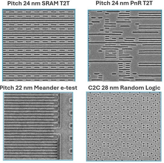
Imec has pushed CAR resists to 22nm-pitch High-NA EUV patterning. The single-exposure work also reaches 28nm-spaced vias for A14/A10 logic.
-
NanoBridge has adopted Siemens synthesis software for two FPGA families. The OEM agreement provides a device-tuned flow for low-power and harsh-environment programmable logic.
-

MegaChips will embed proteanTecs telemetry into next-generation ASIC and LSI. The collaboration targets power, performance, reliability, and lifecycle visibility from development through deployment.
-
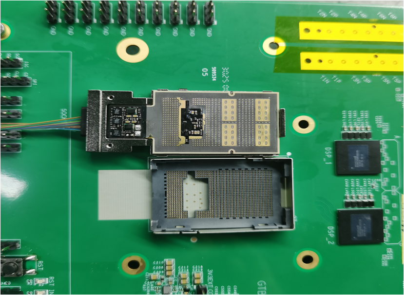
GIGALIGHT has completed a shippable 1.6T near-package optical engineering sample. The socket-based OIF design exposes mechanical and manufacturing barriers that still separate NPO demonstrations from volume deployment.
-

Comcores has appointed AVANT to expand Asian Ethernet IP support. The partnership adds local application engineering for TSN, switching, and security IP across China and Taiwan.
-
Imec has demonstrated denser superconducting circuits using CMOS-compatible 300mm processing. The NbTiN platform reaches 3.8 million Josephson junctions per square centimetre and 30nm routing.
-
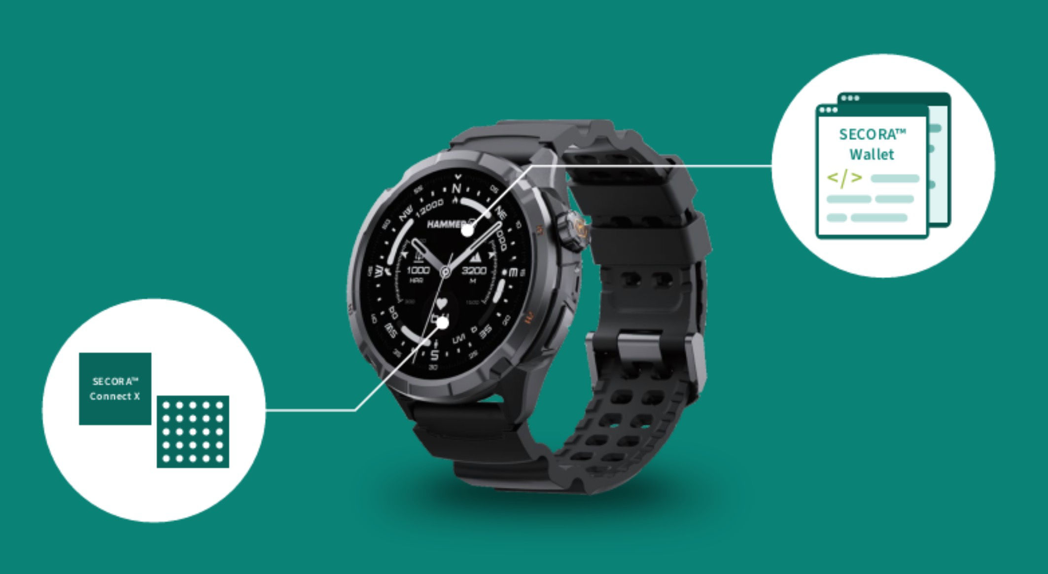
Infineon brings secured NFC payments to mPTech’s latest Hammer smartwatch. The architecture combines embedded security, tokenisation, CDCVM support, and payment-network integration for active wearable devices.
-

Silicon Labs has opened an advanced Austin chip R&D laboratory. The facility adds semiconductor design, test, and validation capability with support from a $23 million Texas Semiconductor Innovation Fund grant.