
Category: Design engineering
-

Rapidus and HCLTech have opened Indian semiconductor development centres together. The Bengaluru and Hubli facilities will support mask design, process design kits, and layout work for advanced manufacturing.
-
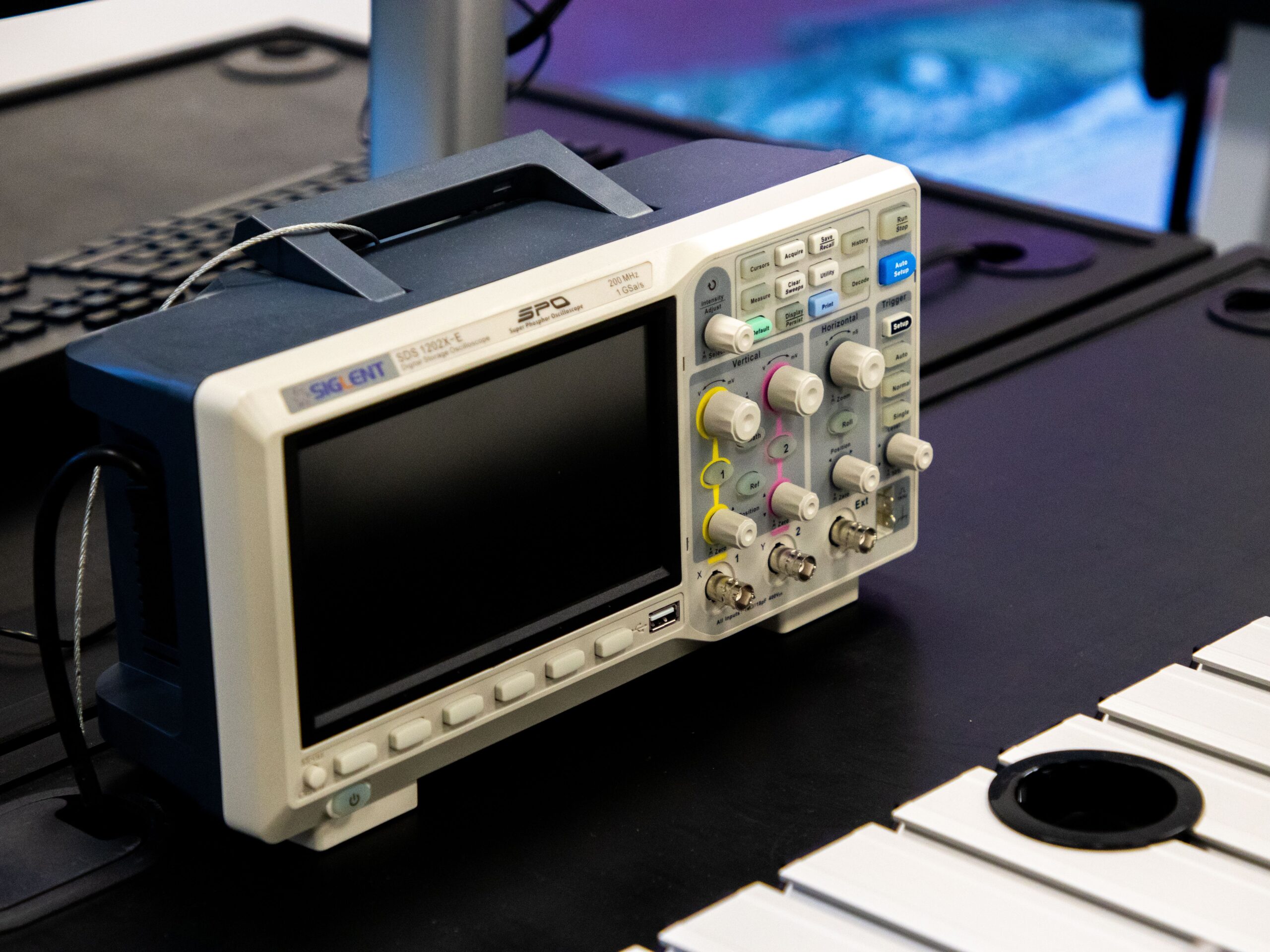
Rohde and Schwarz will introduce two instruments at electronica 2026. The handheld combi analyser combines RF measurement modes, while the HMP5050 offers five independent bench-supply channels.
-

Luxonis has developed modular hardware for multichannel embedded vision applications. The OAK 4 FFC board is intended for system builders integrating several camera channels into robotics and machine equipment.
-

SkyWater is offering quantum photonics startups new semiconductor foundry access. OnRamp provides engineering roadmaps and conditional access to SP90 silicon nitride photonics development runs.
-
Infineon is embedding silicon carbide devices directly within inverter boards. Its ENDOPACK concept targets lower parasitics and a different manufacturing route for automotive power stages.
-

IQE and Atomera have agreed joint RF semiconductor development work. The companies will optimise gallium nitride epitaxy on silicon incorporating Mears Silicon Technology, with wafer samples intended for future customer evaluation.
-

Rambus is adopting ChipAgents across its semiconductor design workflows companywide. The collaboration covers chip and silicon IP development, verification, and AI-assisted integration in existing electronic design automation environments.
-

Glasgow researchers will lead a new UK electronic materials network. The £1.4 million RaRE initiative connects more than 50 partners working on semiconductor processing, electromagnetic materials and sustainable electronics.
-

Cadence has opened sovereign infrastructure for European semiconductor design workloads. Its Munich OnCloud service is available now, with further NVIDIA computing systems and digital twin instances planned.
-
Tenstorrent has released reusable infrastructure for open chiplet integration projects. The beta includes hardware security, system management, debug interfaces and an AXI4-over-UCIe bridge, whose public RTL remains at evaluation quality.