
Category: Design engineering
-

Innolux has unveiled Chip-Last FOPLP for advanced semiconductor packaging production. Its HIPoS platform uses 620 × 670mm panels and targets 2/2µm redistribution-layer geometry ahead of planned 2027 mass production.
-

GlobalFoundries and RAAAM have taped out GCRAM test silicon successfully. Their FDX implementation targets 40% less memory area and power reductions reaching 60% against conventional SRAM.
-

IDS is expanding industrial vision across cameras, AI, and 3D. VISION 2026 demonstrations span event-based sensing, embedded multicamera processing, time-of-flight depth capture, and edge inference.
-

SomDevices modules are joining CELUS to simplify embedded architecture decisions. Seven NXP-based μSMARC variants will become reusable design blocks supporting earlier interface, schematic, and bill-of-material decisions.
-
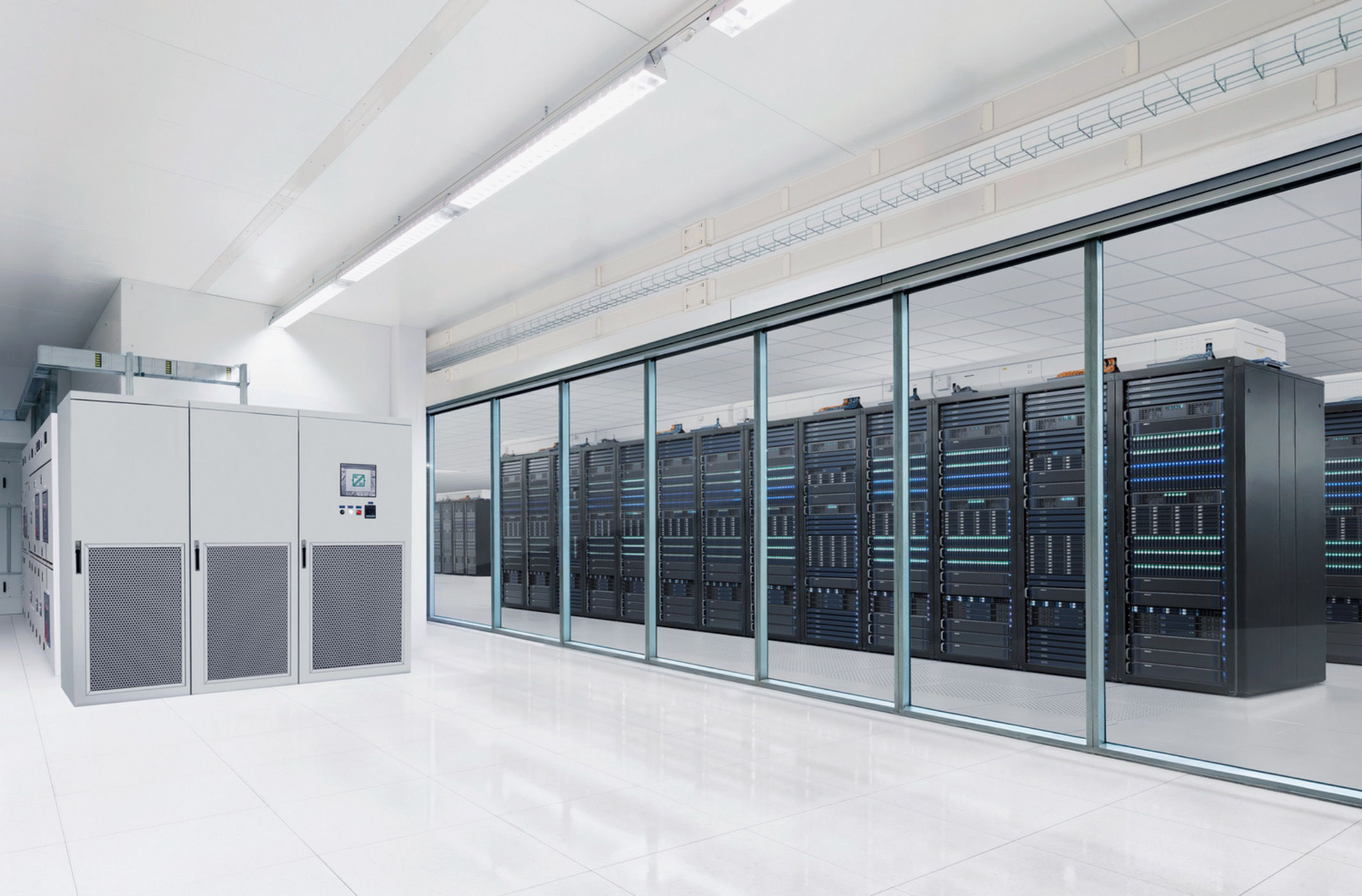
Infineon and Skeleton will develop denser AI power delivery systems. Their MoU covers SiC solid-state transformers and GaN peak-shaving sidecars using supercapacitor storage.
-
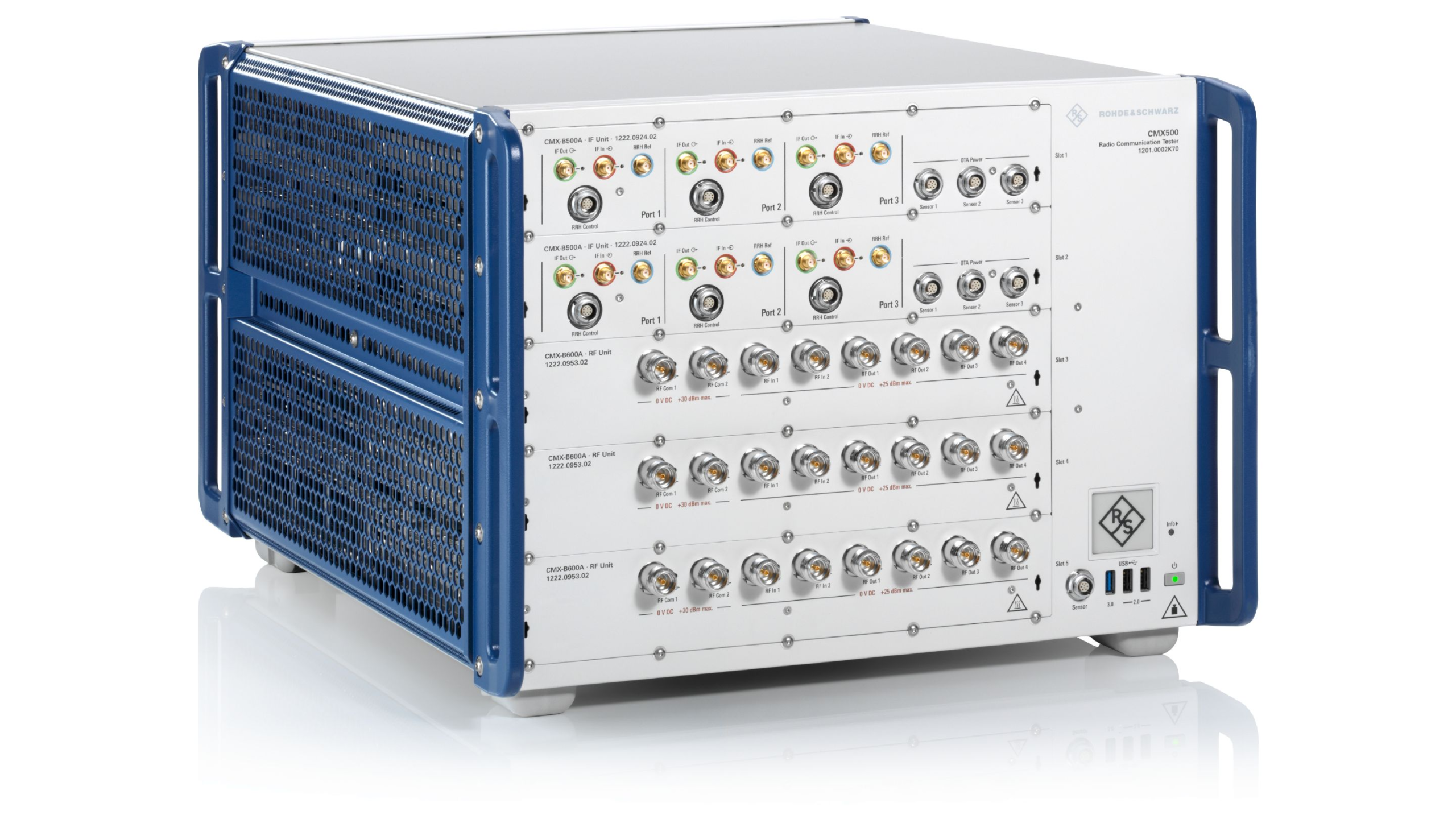
A Release 17 power-saving conformance test has passed initial verification. Rohde & Schwarz and Qualcomm Technologies have moved SSSG closer to formal 5G NR certification.
-
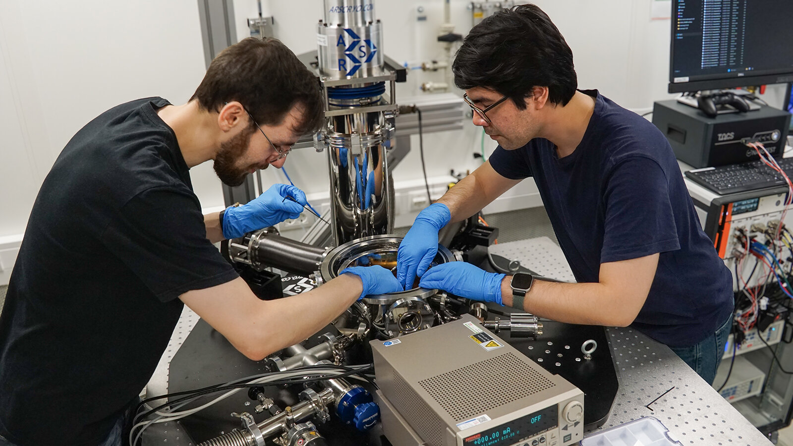
Fraunhofer has opened a cryogenic electronics laboratory in Chemnitz, Germany. CRYME extends semiconductor reliability testing to 4 K for quantum and heterogeneous integration research.
-
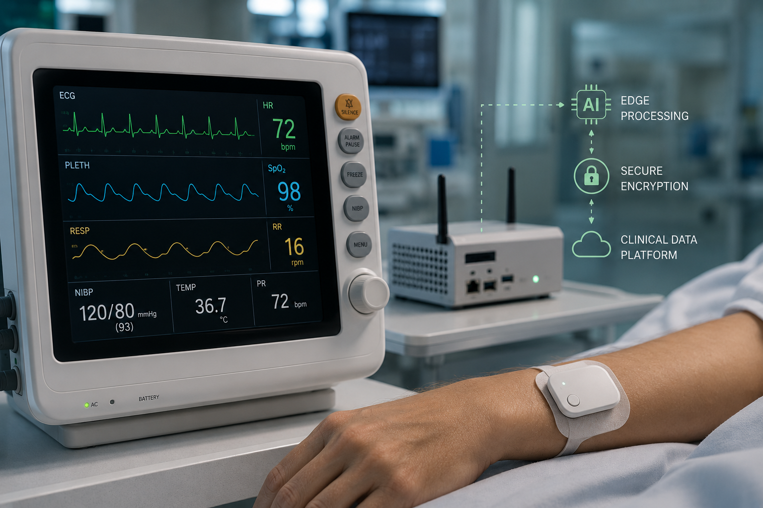
Butterfly is licensing ultrasound-on-chip technology for less-invasive neural interface research. Merge Labs will use the Poseidon family under a multi-year commercial agreement.
-
MediaTek has expanded NVLink Fusion work for custom accelerator programmes. The collaboration adds advanced packaging, HBM integration, rack-scale interconnect, and a $3.5 billion investment.
-
Teradyne has added three instruments for advanced AI semiconductor testing. UltraFLEXplus gains deeper digital patterns, PCIe Gen6 coverage, and multi-kiloamp power delivery.