
Category: Electronics
-
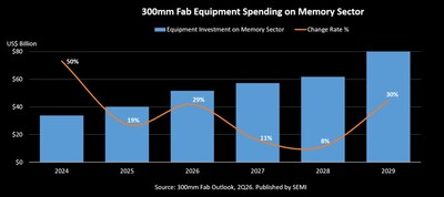
Memory capital spending is being pulled upward by AI demand. SEMI expects 300mm memory equipment investment to exceed $50bn in 2026, with DRAM and 3D NAND spending rising sharply.
-
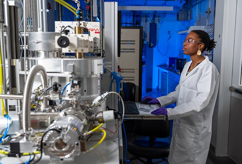
Diamond semiconductor quality control is becoming faster and reproducible now. Rice University researchers have automated defect measurement using Python software and high-resolution X-ray diffraction data.
-
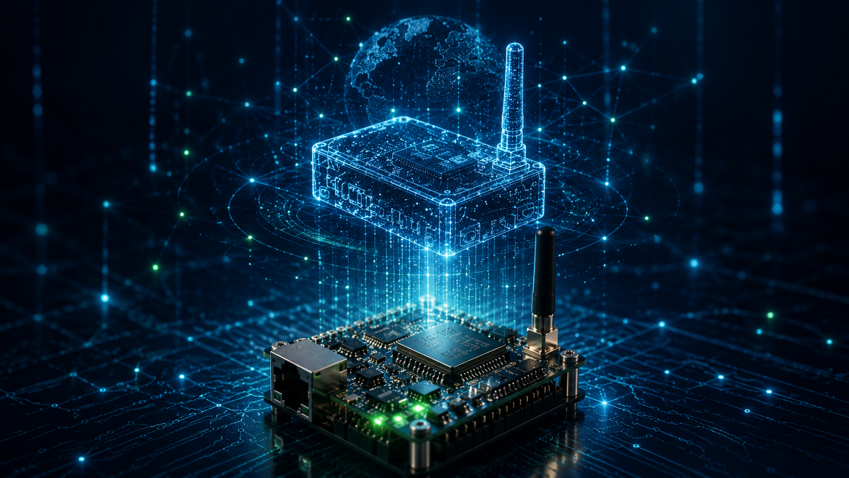
AI infrastructure management is becoming a rack-level electronics discipline now. KAYTUS has launched KSManage Ultra to monitor compute, power, networking, cooling, racks, and clusters.
-
Sequencing hardware is becoming a semiconductor sensor problem again today. Roche’s AXELIOS 1 combines SBX chemistry, nanopores, reusable CMOS modules, and near real-time analysis.
-

Power IC integration is moving further onto engineered substrates now. Soitec and ZenSemi will scale 300mm BCD-on-SOI production for AI, EV, robotics, storage, and industrial systems.
-

Quantum sensing is entering Europe’s semiconductor inspection production chain quickly. QuantumDiamonds will build a Munich test-equipment facility with €76m in German support.
-
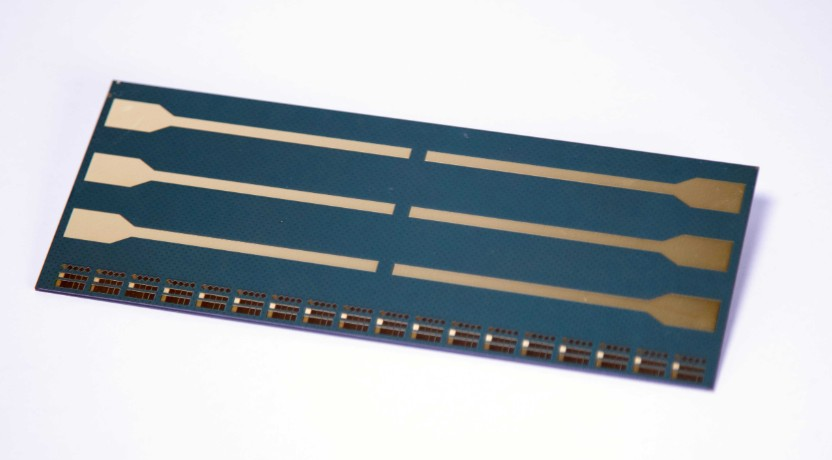
Thintronics has been recognised for low-loss dielectric materials development work. Its materials target boards, packages, and semiconductor interconnect structures.
-
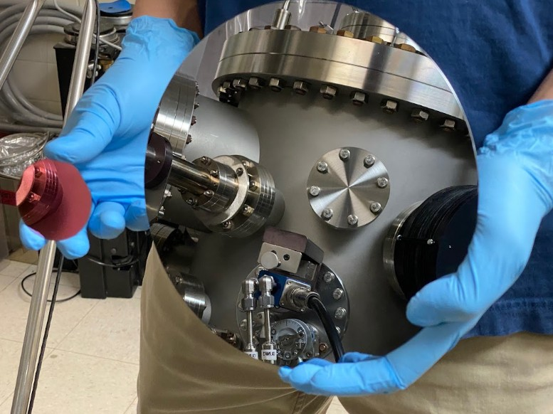
La Luce Cristallina releases beta 200mm wafers for photonics evaluation. The BaTiO₃ platform targets low-voltage electro-optic modulator designs.
-

Incap has added cleanroom assembly capability at its Slovak facility. The Námestovo site now supports ISO 6–7 controlled electronics production.
-
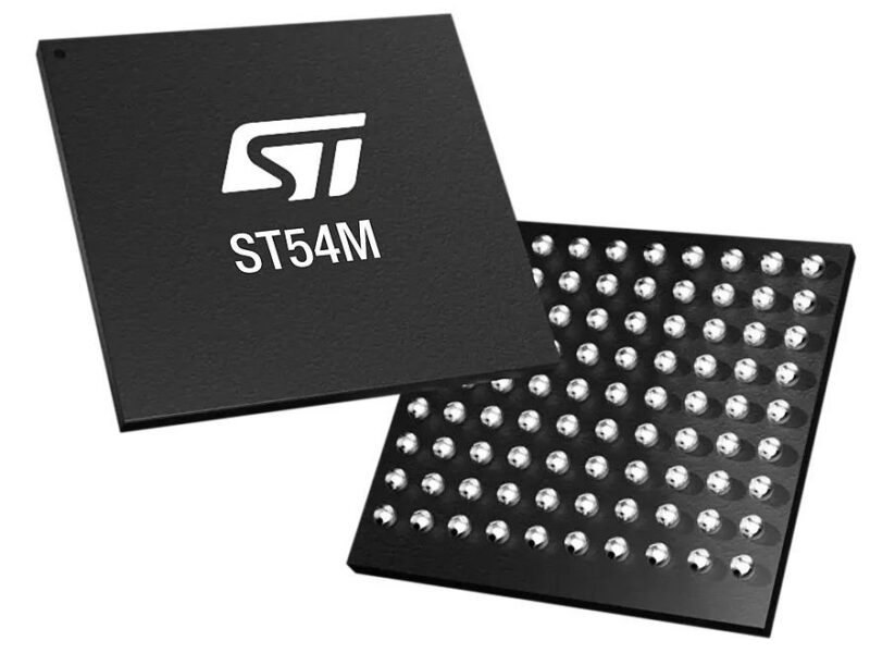
STMicroelectronics has introduced secure silicon for post-quantum mobile services integration. ST54M combines NFC, eSIM, embedded secure element, and cryptographic acceleration in one die.