
Category: News
-
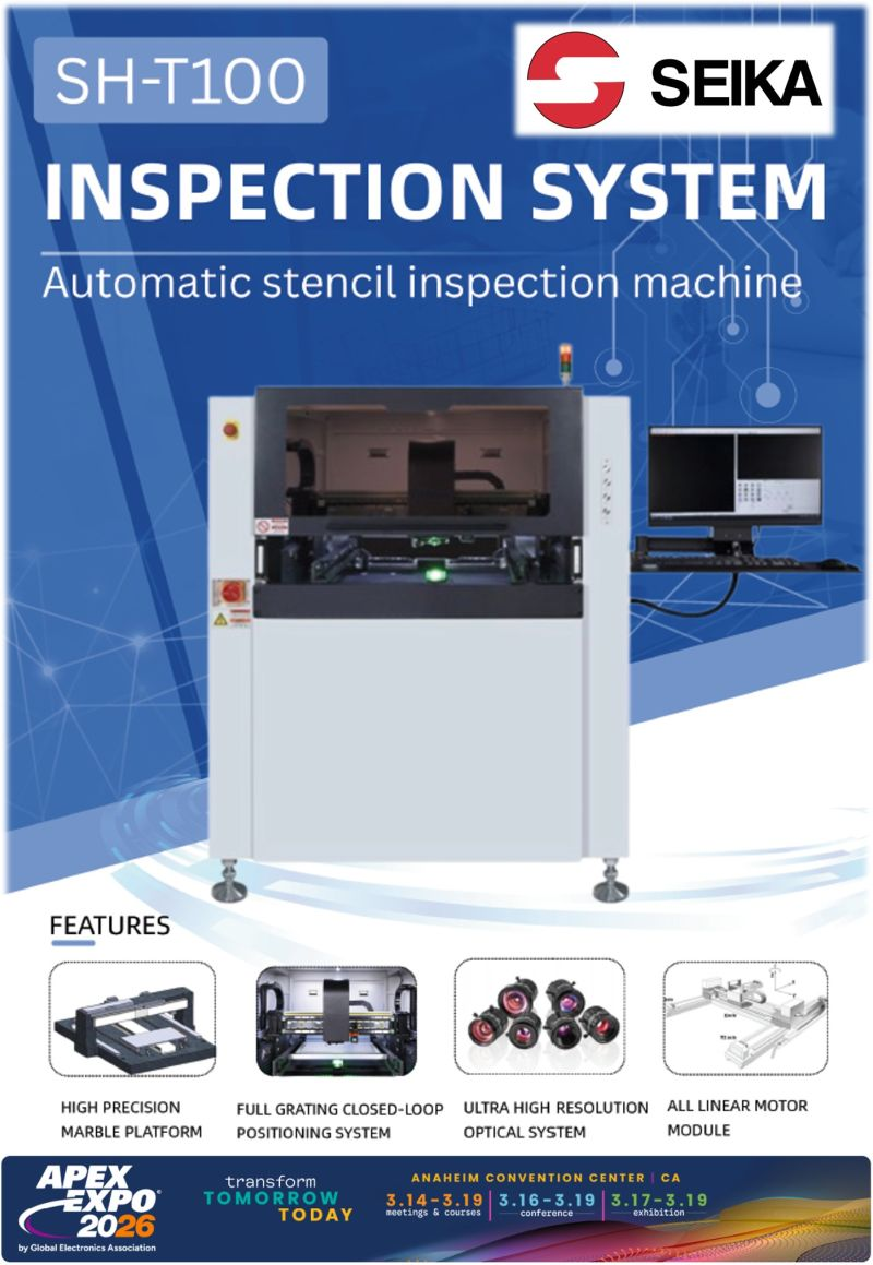
Seika details stencil measurement research at Rochester Institute of Technology. Its operating Sawa T100 inspection system supports comparative testing of stencil geometry and repeatability for ultra-high-density electronics assembly.
-

Valeo and Anritsu have expanded virtual connectivity testing for vehicles. Their combined digital twin environment adds eCall scenarios to simulated cellular networks and virtual electronic control units.
-

VIAVI introduces programmable navigation hardware combining inertial sensors and AI. Its INS-NV platform integrates NVIDIA processing, GNSS reception and interfaces for external aiding sensors, allowing developers to evaluate alternative navigation methods.
-

Rambus is adopting ChipAgents across its semiconductor design workflows companywide. The collaboration covers chip and silicon IP development, verification, and AI-assisted integration in existing electronic design automation environments.
-
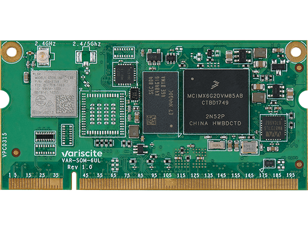
Variscite and SecEdge now support firmware TPM on embedded modules. SEC-TPM runs in a protected environment on supported NXP i.MX processors, allowing security functions without a separate TPM chip.
-
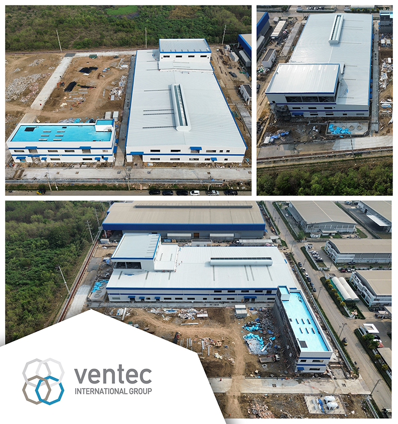
Ventec has opened its first Southeast Asian PCB materials factory. The Thailand operation will progressively expand production of prepreg, bond-ply and laminates, alongside a separate US$50 million investment in Kunshan.
-
Automotive developers report substantial effort spent integrating foundational software systems. A QNX-commissioned survey of 1,100 developers finds that integration absorbs an average 35% of their reported working time.
-

Glasgow researchers will lead a new UK electronic materials network. The £1.4 million RaRE initiative connects more than 50 partners working on semiconductor processing, electromagnetic materials and sustainable electronics.
-

CORE-emt is building larger facilities for Nordic electronics manufacturing customers. Its new Aars headquarters will house equipment demonstrations, practical training and service support, with relocation targeted for March 2027.
-
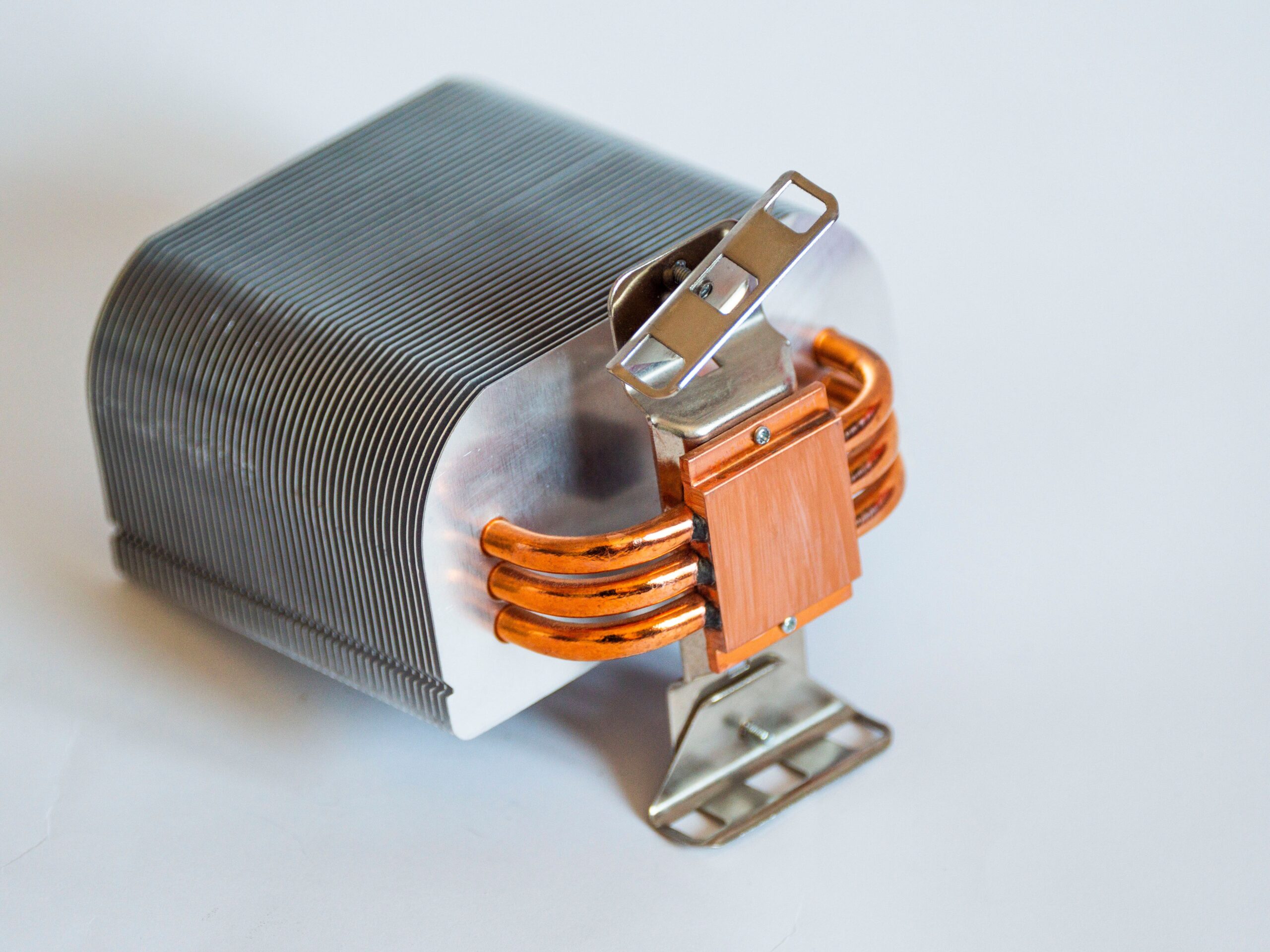
CTX has expanded thermal interface options for electronic cooling assemblies. Its cut-to-size pads, gap fillers and graphite foils can be supplied separately or preassembled with heatsinks.