
Category: Markets
-

Synopsys reported stronger quarterly growth led by Design Automation sales. Third-quarter revenue reached $2.477 billion as EDA, Ansys engineering software, and design IP supported higher full-year expectations.
-

Beijing has launched an atomic-scale manufacturing programme for advanced semiconductors. The 2026–28 plan covers etch, deposition, implantation, process software, precision equipment, metrology, pilot facilities, and industrial demonstration.
-
Beijing has launched a three-year AI4Chip semiconductor industry development programme. The plan applies artificial intelligence across IC design, wafer fabrication, packaging, test, equipment, materials, and supporting engineering infrastructure.
-

Aetina has launched a 2U platform for edge AI workloads. The AIP-RQ87 supports Intel Core Ultra processors, PCIe Gen5 expansion, high-power NVIDIA or Qualcomm acceleration, 256GB of DDR5, and a 2,000W maximum loaded configuration.
-

Renesas has opened a Beijing laboratory for physical AI robotics. The facility combines processing, sensing, power, software, control, and system verification as the semiconductor supplier expands its role in complete robot development.
-
AWS and NVIDIA will deploy two million additional GPUs globally. The programme extends through Blackwell Ultra, Rubin and Rubin Ultra hardware, Vera CPUs, NVLink Fusion, custom high-bandwidth memory, government infrastructure, and robotics.
-
SK hynix has broken ground on its Indiana HBM facility. The $4 billion project combines advanced packaging, testing, and an R&D testbed, with cleanroom opening targeted for 2028 and mass production in 2029.
-

Lam Research has started building its new Oregon semiconductor laboratory. The 120,000ft² project expands cleanroom capacity, deposition and etch development, materials work, and hardware validation.
-
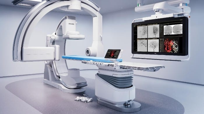
Philips has secured funding for robotic stroke intervention development work. The programme combines image-guided therapy, steerable robotics, and AI-enabled automation to extend specialist thrombectomy capability.
-

Kitron has opened new electronics manufacturing capacity in southern Norway. The 7,500m² Longum plant supports rising defence and aerospace demand while expanding high-reliability production close to European customers.